

Methods for fabricating a stressed MOS device
a stress-induced mobility and device technology, applied in the direction of basic electric elements, semiconductor devices, electrical equipment, etc., can solve the problems of mechanical stability of the sige layer, deterioration of device performance, and reduction of stress-induced mobility
- Summary
- Abstract
- Description
- Claims
- Application Information
AI Technical Summary
Problems solved by technology
Method used
Image

Examples
Embodiment Construction
[0007] The following detailed description is merely exemplary in nature and is not intended to limit the invention or the application and uses of the invention. Furthermore, there is no intention to be bound by any expressed or implied theory presented in the preceding technical field, background, brief summary or the following detailed description.
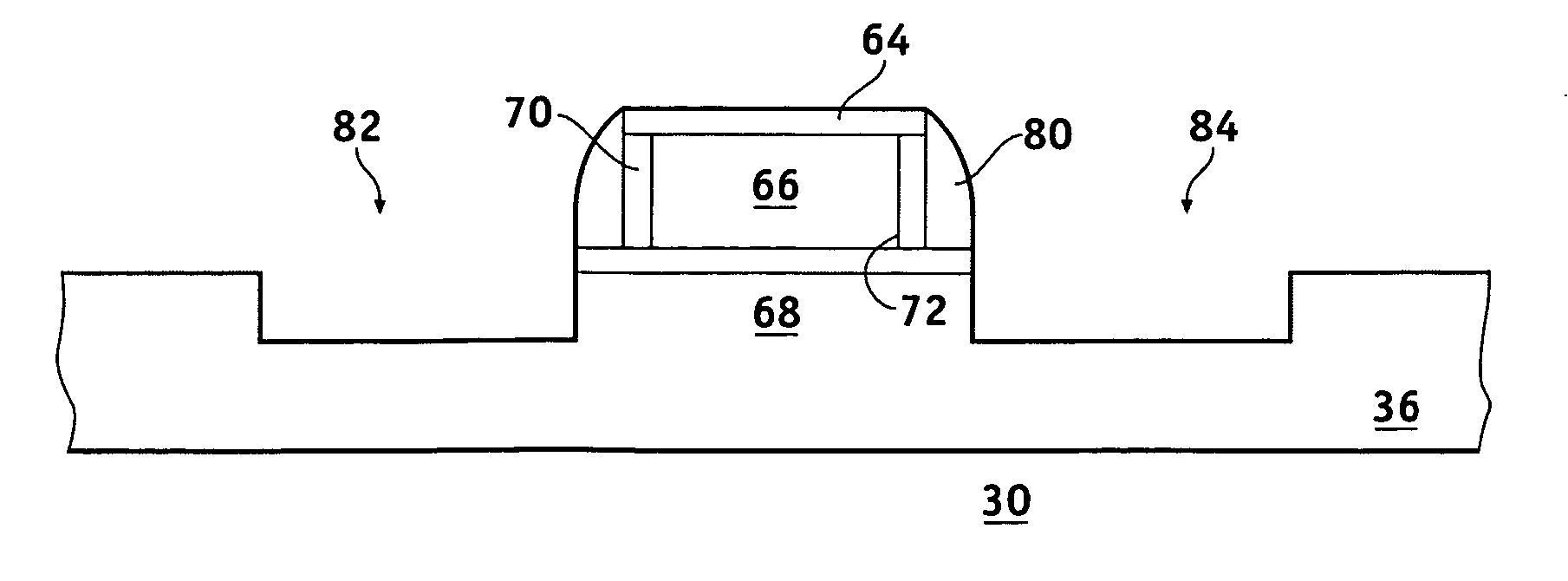
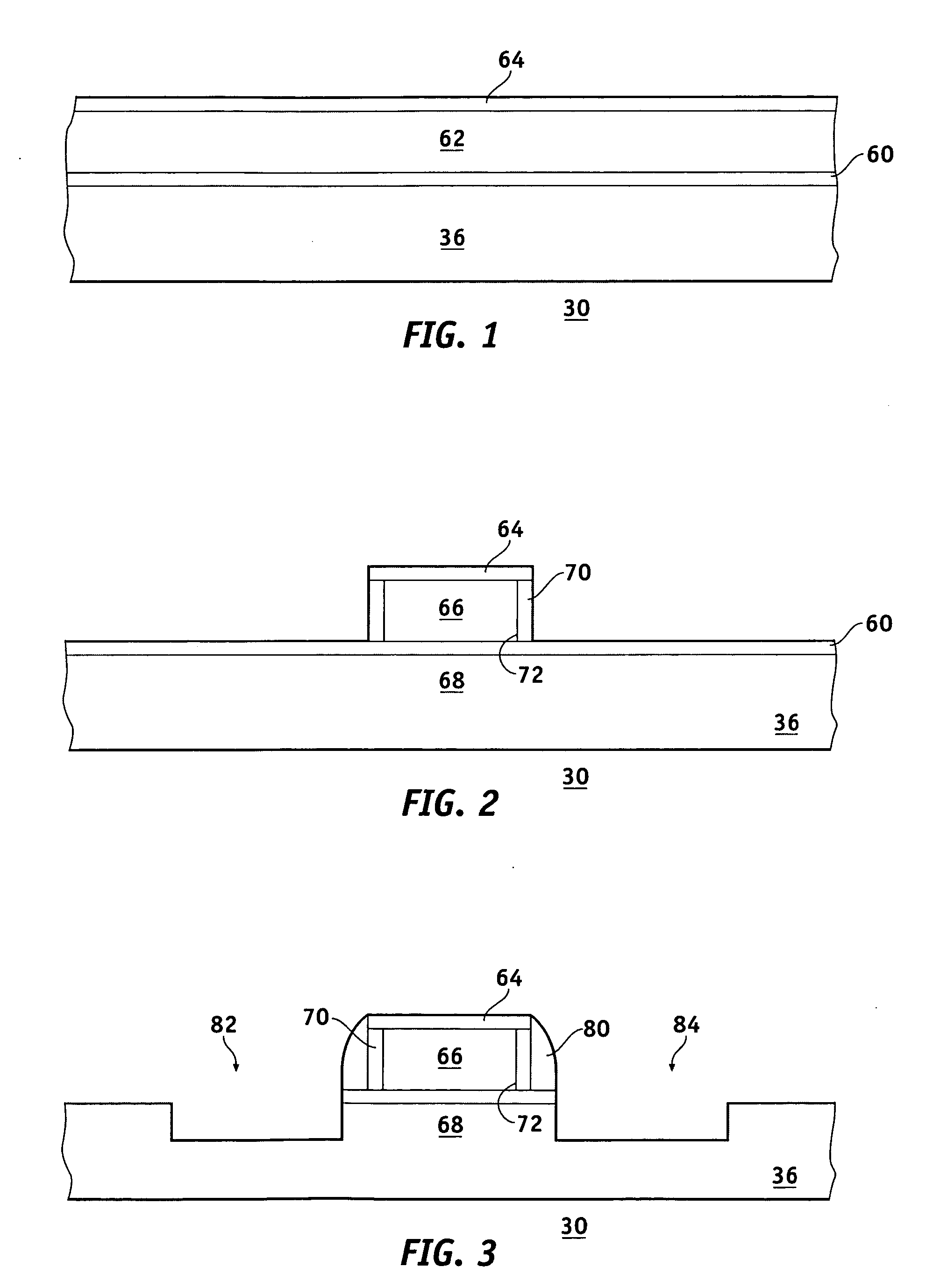
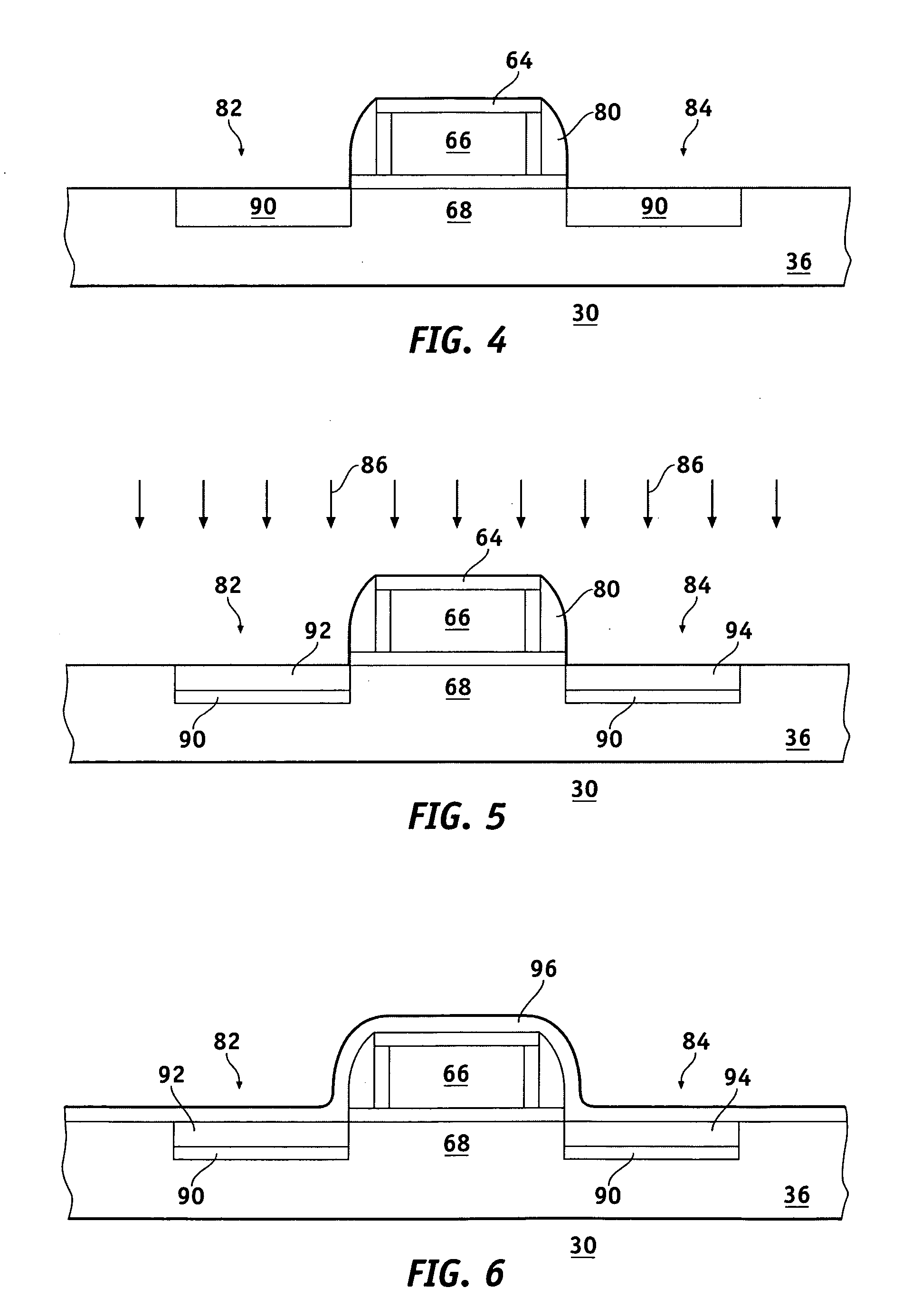
[0008]FIGS. 1-6 illustrate a stressed MOS device 30 and method steps for fabricating such an MOS device in accordance with various embodiments of the invention. In this illustrative embodiment stressed MOS device 30 is illustrated by a single P-channel MOS transistor. An integrated circuit formed from stressed MOS devices such as device 30 can include a large number of such transistors, and may also include unstressed P-channel MOS transistors and stressed and unstressed N-channel transistors as well.
[0009] Various steps in the manufacture of MOS transistors are well known and so, in the interest of brevity, many conventional steps will...
PUM
 Abstract
Description
Claims
Application Information