Increased drive current by isotropic recess etch

a technology of isotropic recess and drive current, which is applied in the direction of semiconductor devices, electrical devices, transistors, etc., can solve the problems of increasing scattering, reducing the mobility advantages associated with strained channels, and reducing the relaxed sige layer. achieve the effect of improving carrier mobility and mobility

Active Publication Date: 2006-06-13
TEXAS INSTR INC
View PDF10 Cites 62 Cited by
  • Summary
  • Abstract
  • Description
  • Claims
  • Application Information

AI Technical Summary

Benefits of technology

[0008]The present invention relates to a device and method of fabrication, wherein a transistor device exhibits improved mobility due to the application of stress to the channel. The device has a stress application region formed in the semiconductor body near the channel region; consequently, less stress inducing species is needed to obtain the desired strain within the channel, thereby providing improved carrier mobility without a substantial number of threading dislocation defects.
[0009]The stress inducing regions in the semiconductor body are formed by selective epitaxial deposition of a silicon germanium material within recesses formed in the body. The recesses are formed using an isotropic etch, wherein the etched recess extends laterally toward the channel region underlying the gate. In one example, the recesses are formed in extension regions prior to the formation of source / drain sidewall spacers; in another example, the recesses are formed in the source / drain regions after the formation of the source / drain sidewall spacers. In either case, the isotropic etch employed in forming the recesses provides for the stress inducing material subsequently formed therein to reside more closely to the channel than would otherwise exist with an isotropic etch. Consequently, stress may be applied to the channel in a substantially more efficient manner.

Problems solved by technology

The ability to form a relaxed SiGe layer is important in obtaining an overlying, epitaxially grown, silicon layer under biaxial tensile strain, however the attainment of the relaxed SiGe layer can be costly and difficult to achieve.
A disadvantage of this method is that germanium within the channel portion of the strain layer can migrate into the overlying gate oxide, thereby causing a relatively large interface trap density (DIT), which disadvantageously increases scattering and reduces the mobility advantages associated with the strained channel.

Method used


Image

  • Increased drive current by isotropic recess etch
  • Increased drive current by isotropic recess etch
  • Increased drive current by isotropic recess etch

Examples


Embodiment Construction

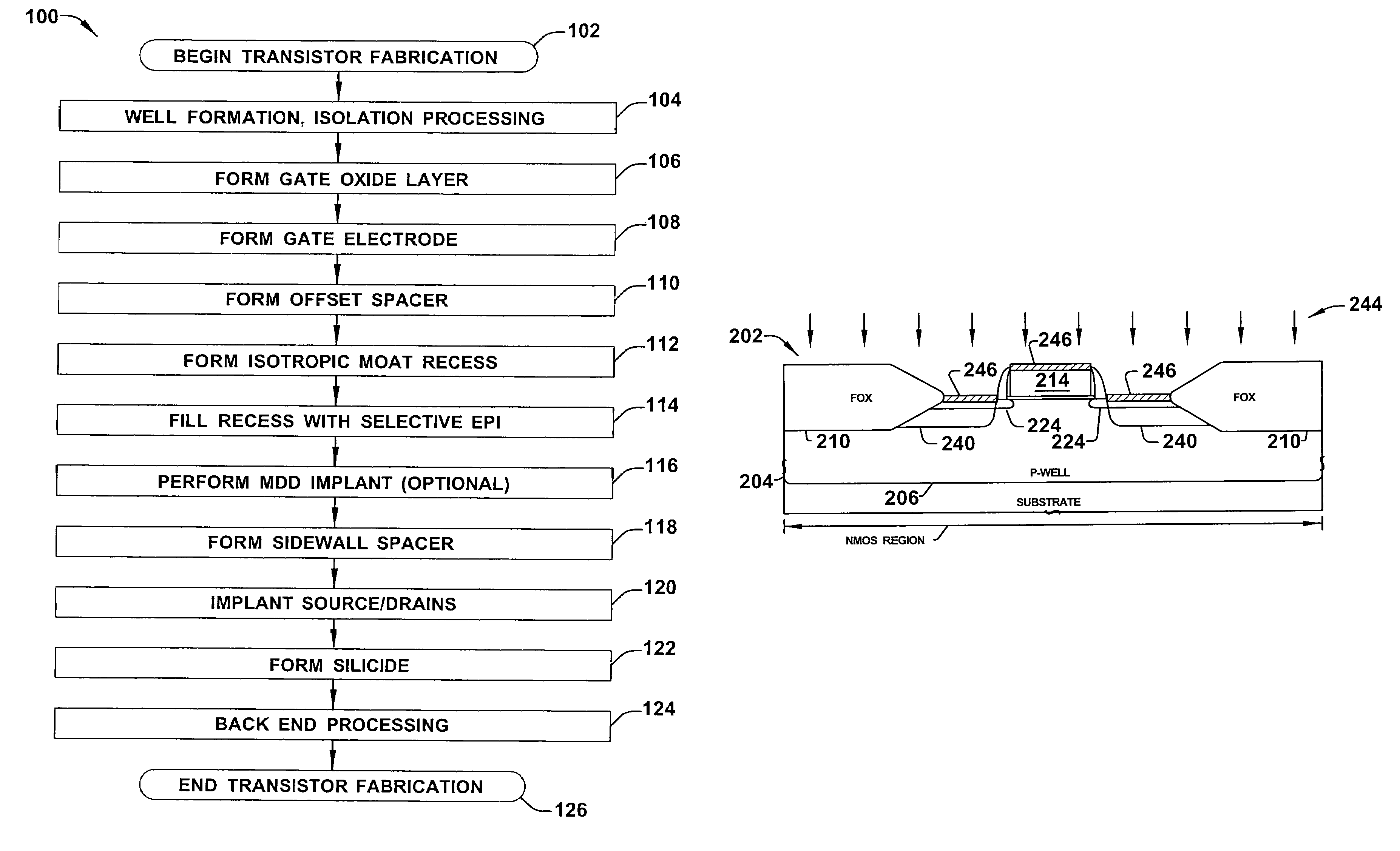
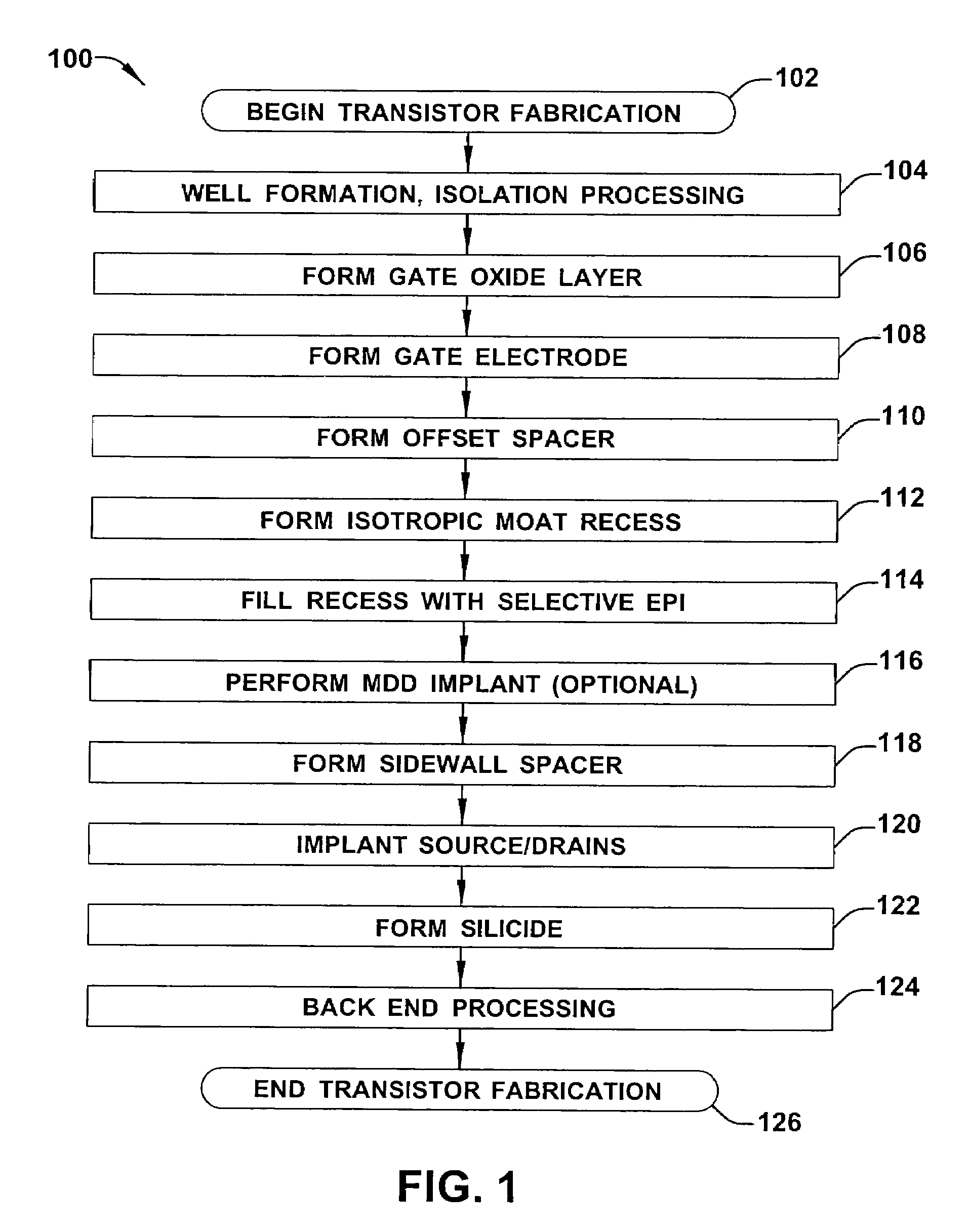
[0017]One or more implementations of the present invention will now be described with reference to the attached drawings, wherein like reference numerals are used to refer to like elements throughout, and wherein the illustrated structures are not necessarily drawn to scale. The invention provides transistor structures and methods in which transistor mobility is improved while minimizing defects heretofore associated with conventional strained silicon device solutions.

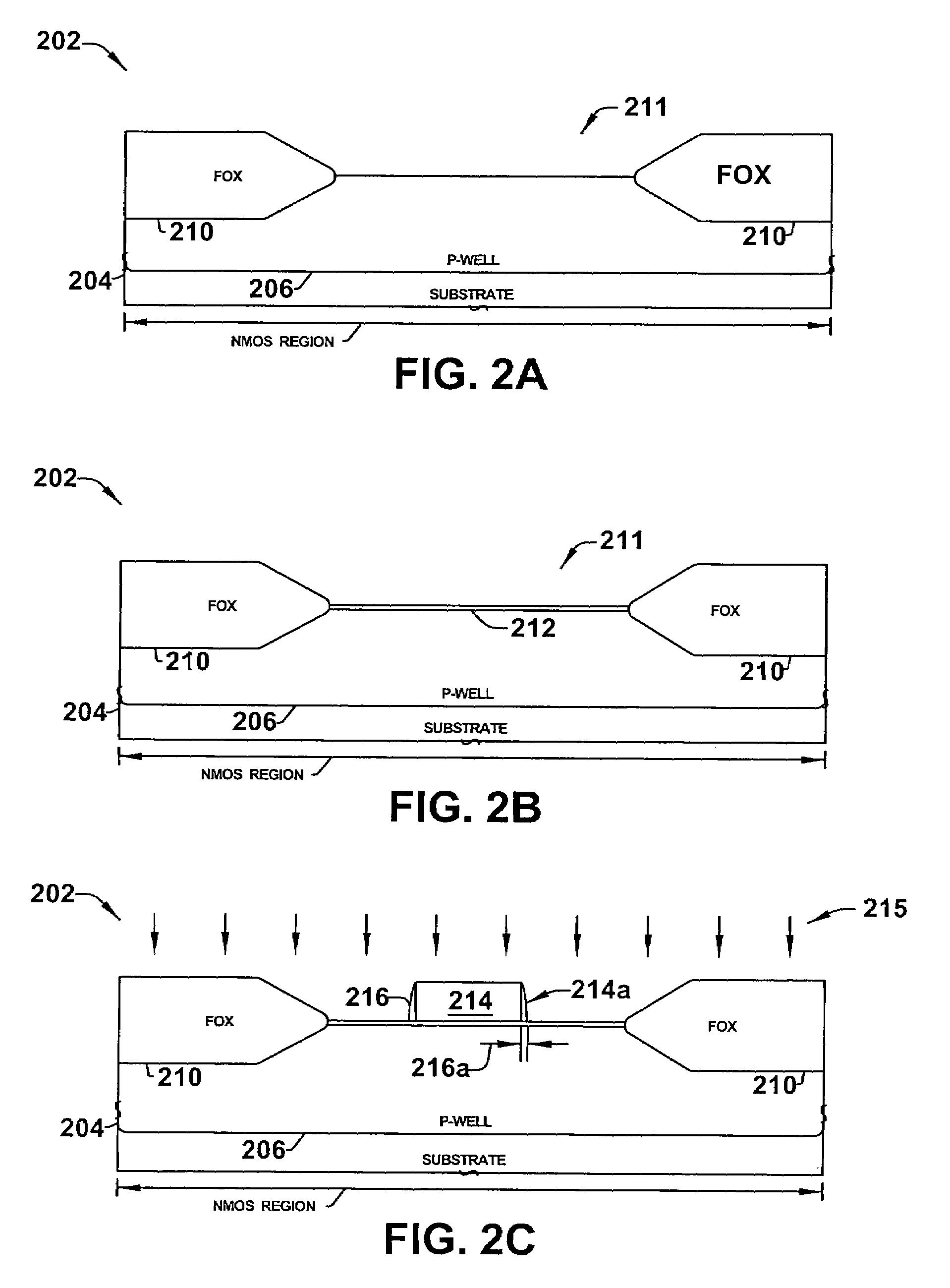
[0018]Referring now to FIGS. 1 and 2A–2G, further aspects of the invention relate to methods of fabricating integrated circuits, wherein FIG. 1 illustrates an exemplary method 100 in accordance with the invention, and FIGS. 2A–2G illustrate the exemplary transistor device at various stages of fabrication in accordance with the invention. While the exemplary method 100 is illustrated and described below as a series of acts or events, it will be appreciated that the present invention is not limited by the illustrated ord...


PUM


Abstract

A method (100) of forming a transistor includes forming a gate structure (108) over a semiconductor body and forming recesses (112) using an isotropic etch using the gate structure as an etch mask. The isotropic etch forms a recess in the semiconductor body that extends laterally in the semiconductor body toward a channel portion of the semiconductor body underlying the gate structure. The method further includes epitaxially growing silicon (114) comprising stress-inducing species in the recesses. The source and drain regions are then implanted (120) in the semiconductor body on opposing sides of the gate structure.

Description

FIELD OF INVENTION[0001]The present invention relates generally to semiconductor devices and more particularly to transistors and associated methods of manufacture having improved mobility due to channel strain.BACKGROUND OF THE INVENTION[0002]A conventional MOS transistor generally includes a semiconductor substrate, such as silicon, having a source, a drain, and a channel positioned between the source and drain. A gate stack composed of a conductive material (a gate conductor), an oxide layer (a gate oxide), and sidewall spacers, is typically located above the channel. The gate oxide is typically located directly above the channel, while the gate conductor, generally comprised of polycrystalline silicon (polysilicon) material, is located above the gate oxide. The sidewall spacers protect the sidewalls of the gate conductor.[0003]Generally, for a given electric field across the channel of a MOS transistor, the amount of current that flows through the channel is directly proportiona...

Claims


Application Information

Patent Timeline
Patent Type & Authority Patents(United States)
IPC IPC(8): H01L21/336H01L21/3205H01L21/4763H01L21/76
CPCH01L29/6656H01L29/7833H01L29/66636H01L29/6659H01L29/665
Inventor CHIDAMBARAM, PRHALL, LINDSEYBU, HAOWEN
Owner TEXAS INSTR INC
Why Eureka
Try Eureka