

Structure and method to increase strain enhancement with spacerless fet and dual liner process
a spacerless fet and strain enhancement technology, applied in the field of structure and method to increase the strain enhancement of spacerless fet and dual liner process, can solve the problems of resistance of silicide contacts, and achieve the effects of reducing the width of such a spacer, improving device speed, and strengthening strain enhancemen
- Summary
- Abstract
- Description
- Claims
- Application Information
AI Technical Summary
Benefits of technology
Problems solved by technology
Method used
Image

Examples
Embodiment Construction
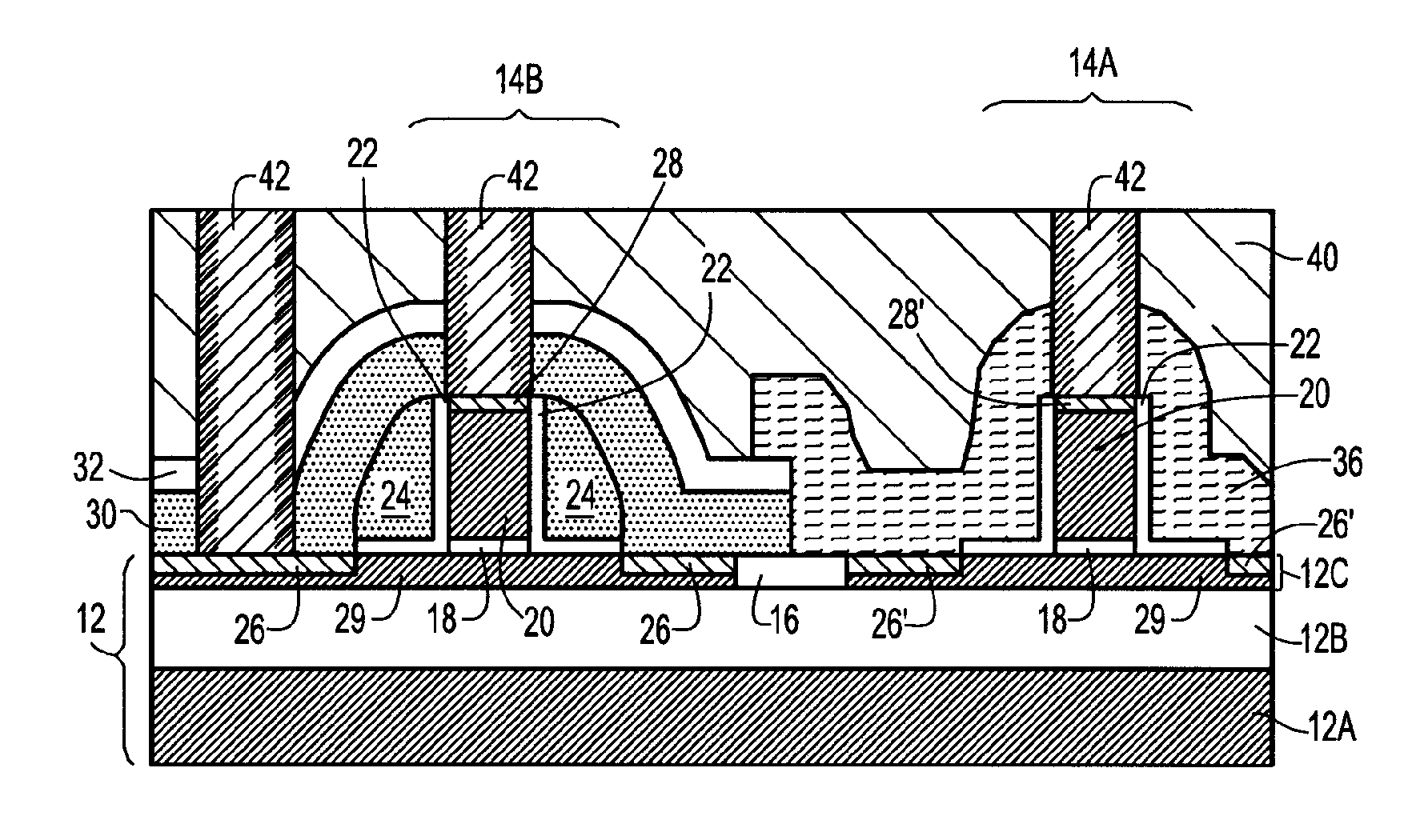
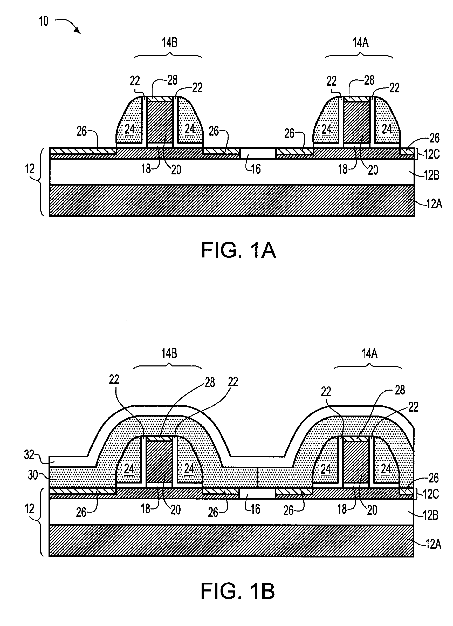
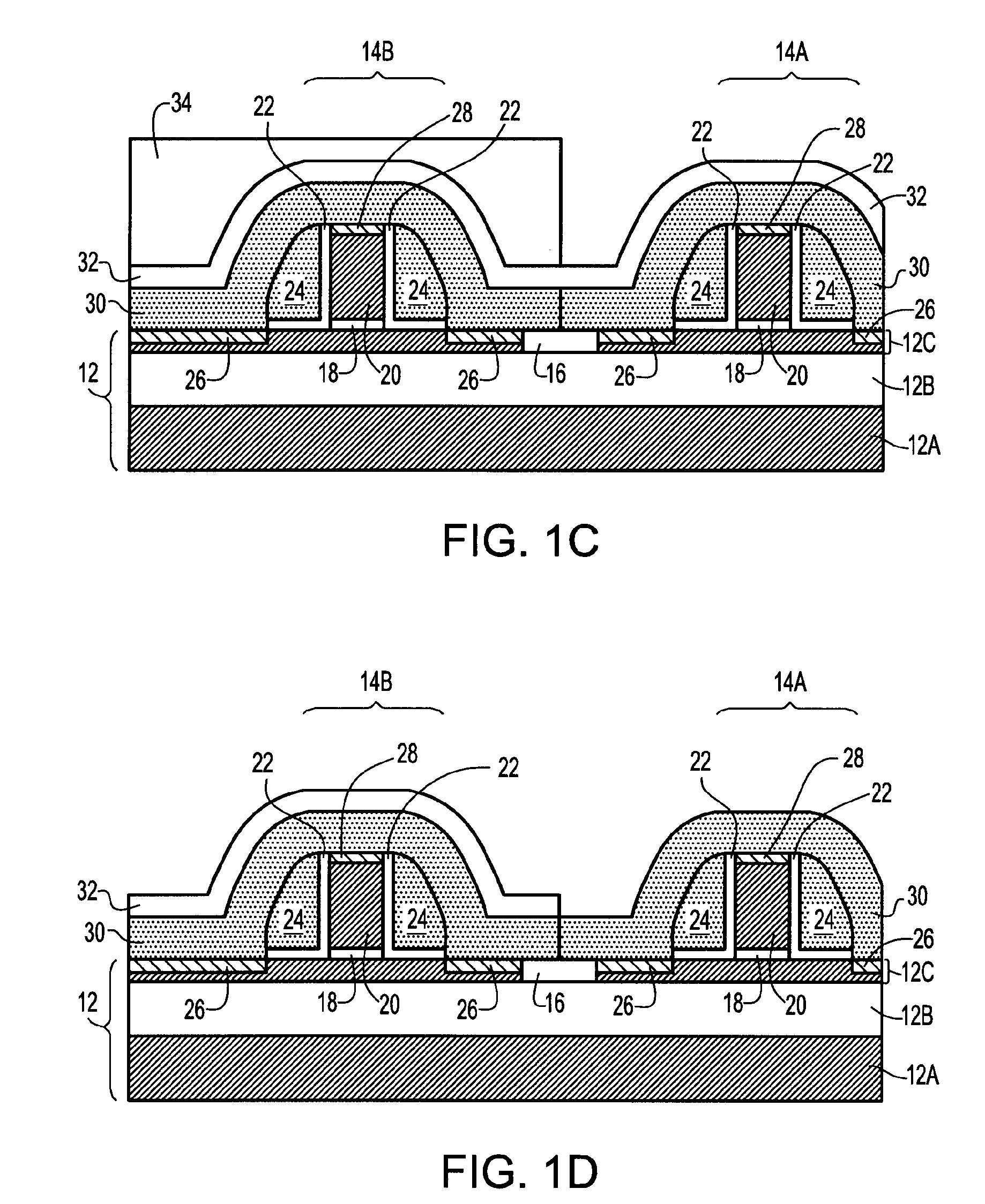
[0031] The present invention, which provides a structure and method to increase strain enhancement for FET devices, will now be described in greater detail by referring to the following discussion and drawings that accompany the present application. It is noted that the drawings of the present application are provided for illustrative purposes and, as such, they are not drawn to scale.
[0032] The present invention will now be described in context with a preferred embodiment thereof in which strain enhancement is achieved using a spacerless pFET. Although a spacerless pFET is described and depicted hereinbelow, the present application also contemplates the case where a spacerless nFET is used alone or in conjunction with a spacerless pFET. When only a spacerless nFET is employed, the processing sequence is modified such that a compressive stress inducing liner is first formed, removed from the nFET region, and thereafter the wide spacer is removed from the nFET device. When spacerles...
PUM
 Abstract
Description
Claims
Application Information