Method for mounting a component in or on a circuit board, and circuit board

a technology for circuit boards and components, applied in the direction of printed circuit non-printed electric components association, gas flame welding apparatus, non-electric welding apparatus, etc., can solve the problems of inability to easily ensure or provide sufficient safety and strength of adhesive connections, requiring a comparatively high amount of work input, and requiring a large amount of work inpu

Active Publication Date: 2013-09-12
AT & S AUSTRIA TECH & SYSTTECHN AG
View PDF1 Cites 2 Cited by
  • Summary
  • Abstract
  • Description
  • Claims
  • Application Information

AI Technical Summary

Benefits of technology

[0004]The present invention aims to avoid, or at least reduce, the problems of the known prior art involved in the connection of a metal surface of a component or element to be mounted in or on a circuit board and a conducting layer of a circuit board, wherein it is, in particular, aimed to enable the formation of a reliable and mechanically loadable connection providing proper conductivity.

Problems solved by technology

The soldering of metal surfaces or conducting layers made of metal materials of a circuit board involves the drawback of requiring a comparatively high amount of work input.
Moreover, soldering procedures are partly extremely complex, and partly almost inoperable, especially with planes or surfaces to be connected and consisting of different materials.
When gluing such planes or surfaces to be connected, it is frequently disadvantageous that adhesive connections will not readily ensure or provide sufficient safety and strength under elevated or extended stress.
Besides, a thermally or electrically well conducting adhesive connection is, for instance, not or not readily feasible even when using adhesives having special conductivities.

Method used


Image

  • Method for mounting a component in or on a circuit board, and circuit board
  • Method for mounting a component in or on a circuit board, and circuit board
  • Method for mounting a component in or on a circuit board, and circuit board

Examples


Embodiment Construction

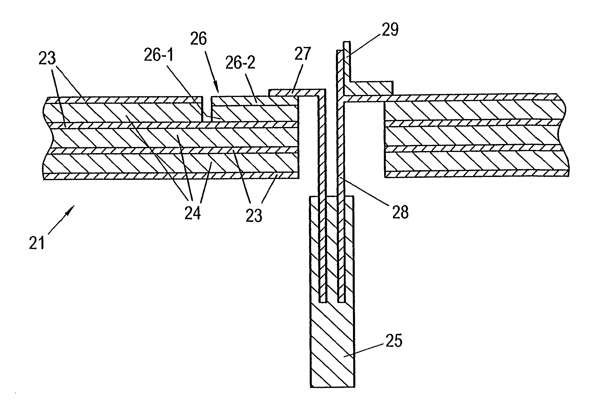
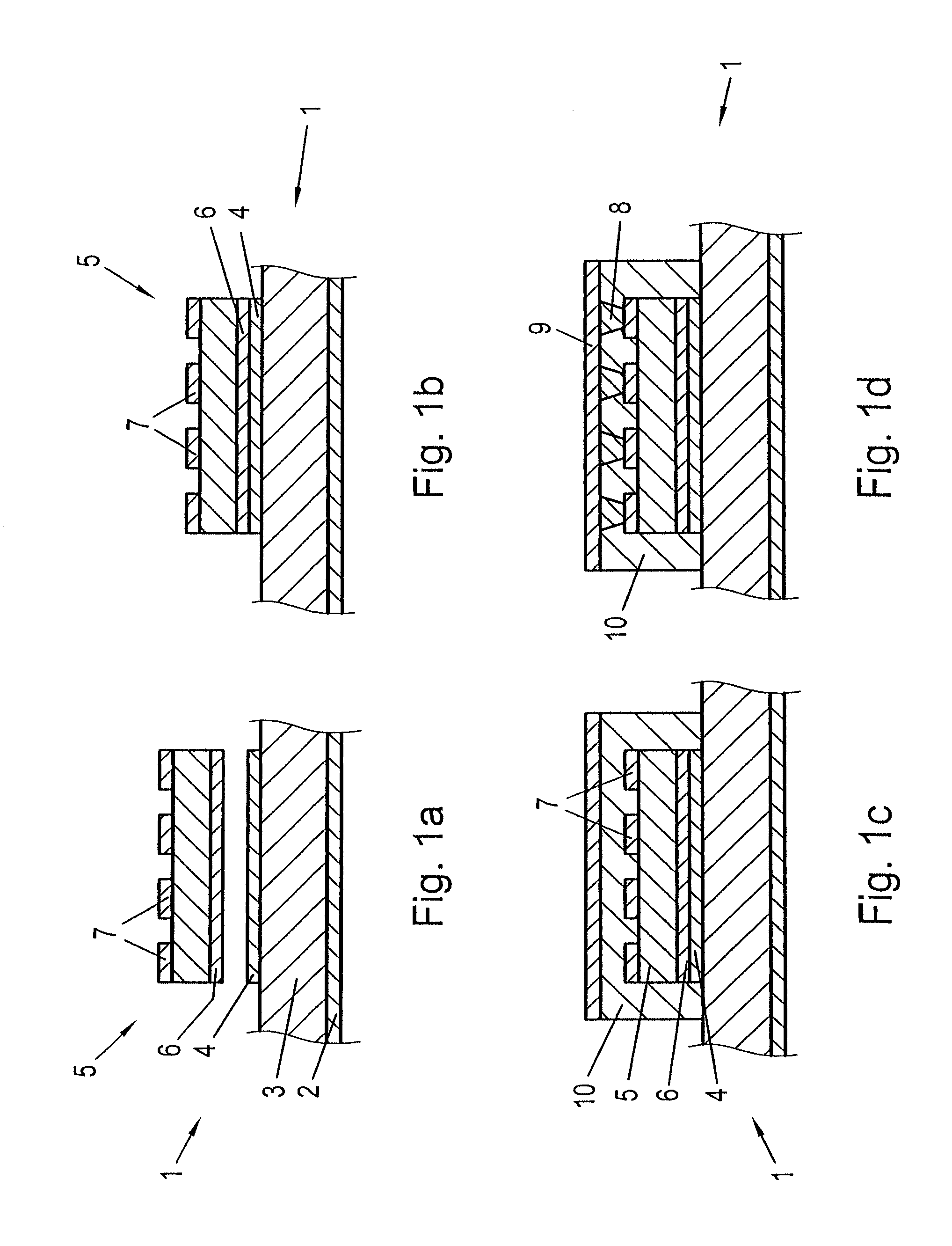
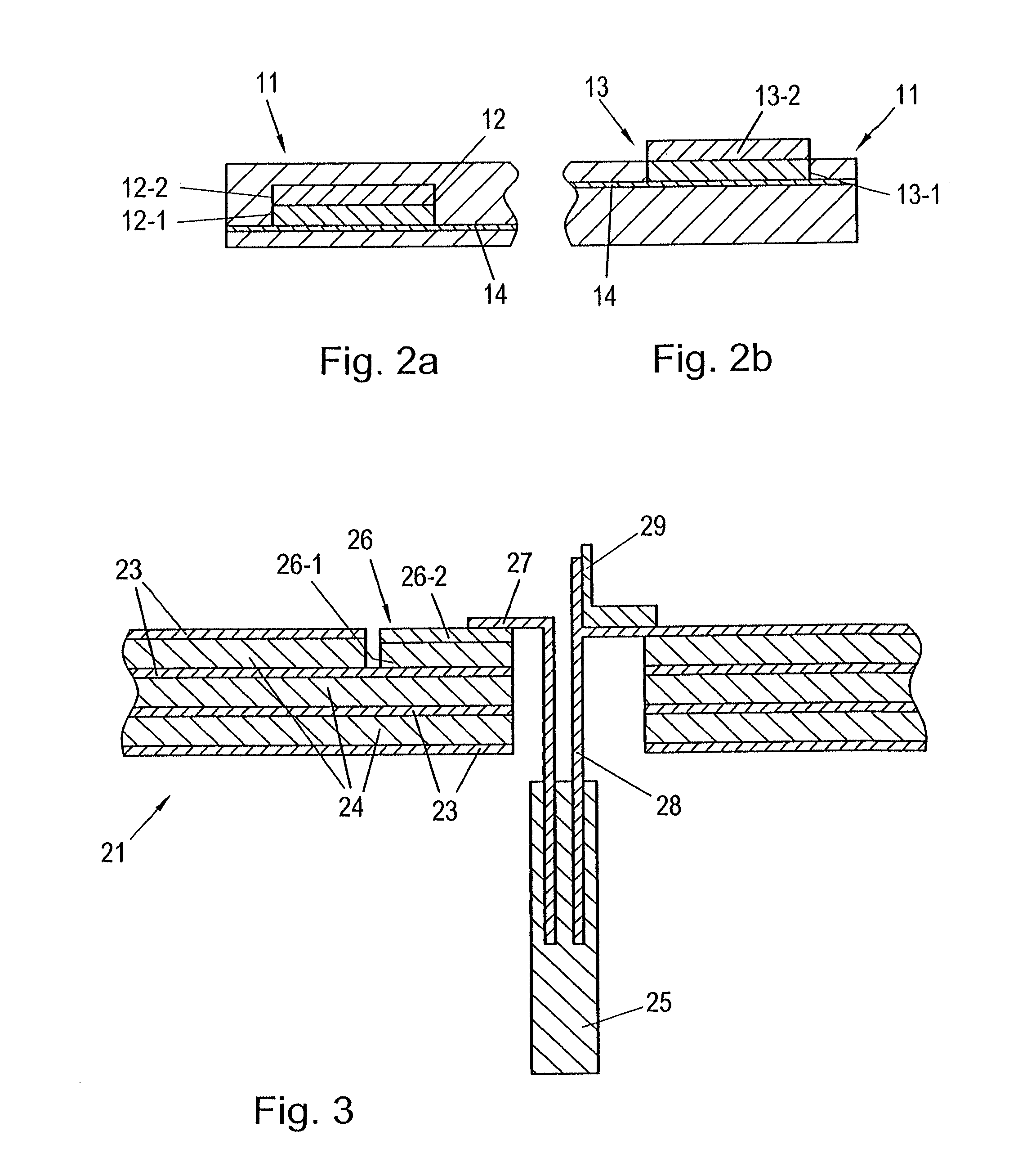
[0025]In FIG. 1, a subarea of a circuit board schematically denoted by 1 is each illustrated, the multilayer structure of the circuit board 1 being merely indicated by the provision of a conducting or conductive layer 2, an insulating or non-conducting layer 3 and a conducting or conductive layer 4, wherein an element or component 5 is to be connected to the subarea of the conducting or conductive layer 4 of the circuit board 1, as will be discussed in more detail below.

[0026]A correspondingly larger number of layer or plies may be provided for the circuit board 1 as a function of the purpose of use or an optionally provided production of the circuit board 1 in preceding production steps not illustrated in detail.

[0027]A connection between the conducting or conductive layer 4 of the circuit board 1 and the component or element 5 between the conducting or conductive layer 4 of the circuit board 1 and a metal surface 6 of the component 5 is made by ultrasonic welding or high-frequency...


PUM

PropertyMeasurementUnit
frequencyaaaaaaaaaa
conductingaaaaaaaaaa
thermal conductivitiesaaaaaaaaaa

Abstract

In a method for mounting an element or component having at least one metal surface in or on a circuit board containing at least one conducting layer made of metal material, a connection between the at least one metal surface of the element and the at least one conducting layer of the circuit board is formed using ultrasonic welding or high-frequency friction welding in order to create a mechanically stable and resistant connection or attachment having good conductivity. Furthermore, a circuit board is disclosed in which at least one element or component having a metal surface is or can be connected to a conducting or conductive layer of the circuit board using ultrasonic welding or high-frequency friction welding.

Description

[0001]This is a national stage of PCT / AT2011 / 000464 filed Nov. 16, 2011 and published in German, which has priority of Austria no. GM 709 / 2010 filed Nov. 19, 2010, hereby incorporated by reference.FIELD OF THE INVENTION[0002]The present invention relates to a method for mounting an element or component having at least one metal surface in or on a circuit board containing at least one conducting layer made of metal material, and a circuit board containing at least one conducting layer made of metal material.PRIOR ART[0003]In the context of mounting an element or component having at least one metal surface in or on a circuit board, various methods such as soldering or gluing are known. The soldering of metal surfaces or conducting layers made of metal materials of a circuit board involves the drawback of requiring a comparatively high amount of work input. Moreover, soldering procedures are partly extremely complex, and partly almost inoperable, especially with planes or surfaces to b...

Claims


Application Information

Patent Timeline
Patent Type & Authority Applications(United States)
IPC IPC(8): H05K3/32H05K1/18
CPCH05K1/142H05K1/181H05K3/4015H05K3/328H01L2224/19H01L2224/04105H01L2224/24H01L2224/32225H01L2224/73267H01L2224/82H01L2224/92244H01L2924/13091H01L2224/06181H01L2924/00H01L2224/18
Inventor WEICHSLBERGER, GUENTHERDROFENIK, DIETMAR
Owner AT & S AUSTRIA TECH & SYSTTECHN AG
Why Eureka
Try Eureka