Al technical title is built by PatSnap Al team. It summarizes the technical point description of the patent document.
a sensing array and capacitive technology, applied in the field of circuits, can solve the problems of limiting the voltage that may be applied to the drive ring, excitation the finger to too high a voltage, and the thickness of any dielectric overlaying the sensor may also be limited
Active Publication Date: 2013-10-17
APPLE INC
View PDF15 Cites 74 Cited by
Summary
Abstract
Description
Claims
Application Information
AI Technical Summary
This helps you quickly interpret patents by identifying the three key elements:
Problems solved by technology
Method used
Benefits of technology
Problems solved by technology
In such a sensor, the voltage that may be applied to the drive ring may be limited.
Voltages above this may excite the finger to too high a voltage; this excessive excitation may be detected by a person as a “tingling” or uncomfortable feeling in their finger.
Since the drive ring's voltage is restricted to avoid user perception, the thickness of any dielectric overlaying the sensor may also be limited.
The thicker the dielectric between sensor pad and finger, the more attenuated the resulting capacitance and the blurrier the fingerprint image becomes.
For dielectrics having a thickness or more than approximately 100 microns, the fingerprint image may become unreliable.
Another limitation arises when other parts of the user's finger or hand or body may capacitively couple through earth ground to the system, or directly to the system ground when touching other parts of the system.
This parasitic coupling attenuates the voltage that the drive ring is able drive into the user's finger, and as such reduces the signal.
Method used
Image
Click on the blue label to locate the original text in one second.
Reading with bidirectional positioning of images and text.
Examples
Embodiment Construction
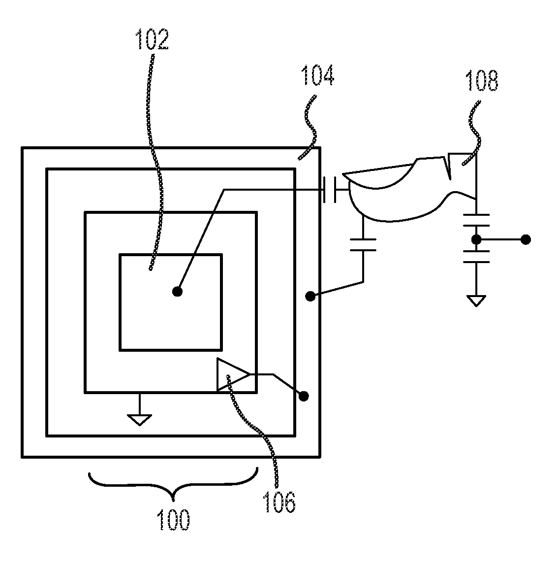
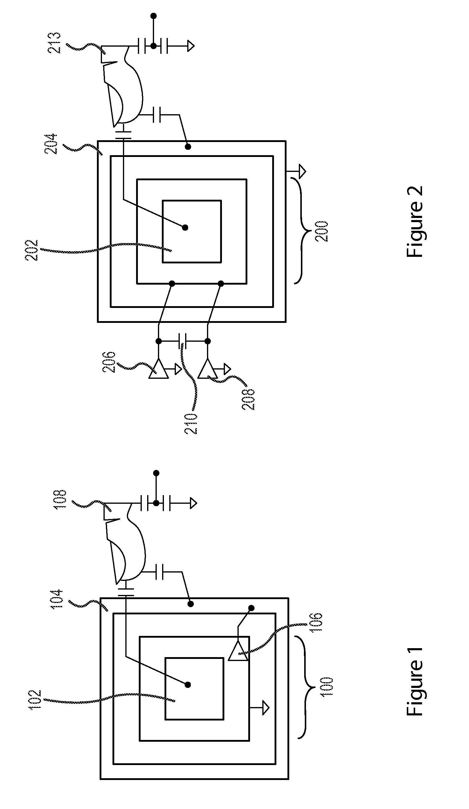
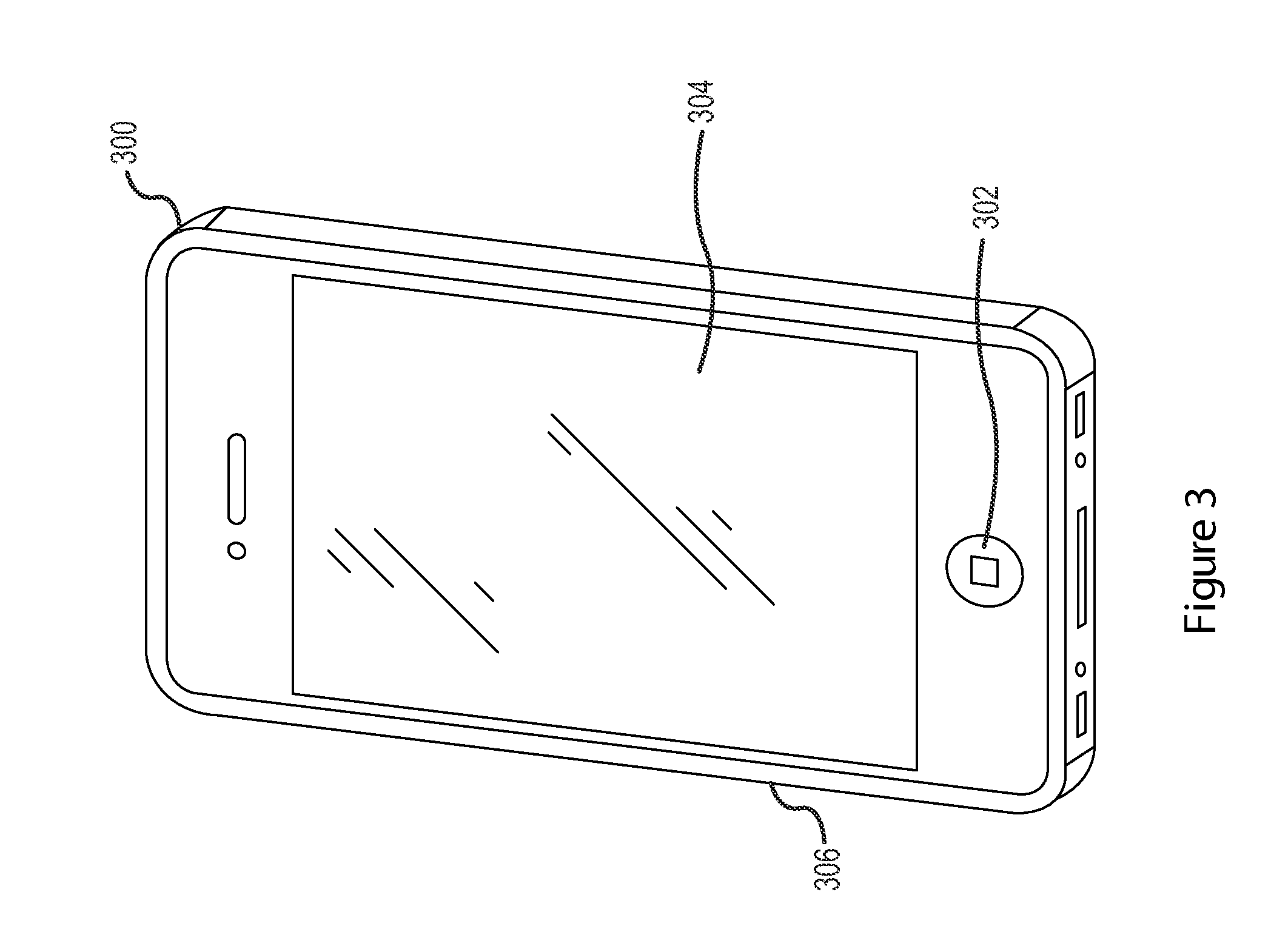
[0021]Generally, embodiments discussed herein may take the form of a capacitive sensor, such as a fingerprint sensor. The sensor may be formed from a capacitive sensing element array; each capacitive sensing element of the array may register a voltage that varies with the capacitance of a capacitive coupling. A finger may capacitively couple to the individual capacitive sensing elements of the sensor, such that the sensor may sense a capacitance between each capacitive sensing element and the flesh of the fingerprint. The capacitance signal may be detected by sensing the change in voltage on the capacitive sensing element as the relative voltage between the finger and the sensing chip is changed. Alternately, the capacitance signal may be detected by sensing the change in charge received by the capacitive sensing elements as the relative voltage between the finger and the sensing chip is changed. Portions of the finger further away from the sensor may create a lower capacitance betw...
PUM
Abstract
A capacitive fingerprint sensor that may be formed of an array of sensing elements. Each capacitive sensing element of the array may register a voltage that varies with the capacitance of a capacitive coupling. A finger may capacitively couple to the individual capacitive sensing elements of the sensor, such that the sensor may sense a capacitance between each capacitive sensing element and the flesh of the fingerprint. The capacitance signal may be detected by sensing the change in voltage on the capacitive sensing element as the relative voltage between the finger and the sensing chip is changed. Alternately, the capacitance signal may be detected by sensing the change in charge received by the capacitive sensing elements as the relative voltage between the finger and the sensing chip is changed.
Description
CROSS-REFERENCE TO RELATED APPLICATIONS[0001]This application claims the benefit under 35 U.S.C. §119(e) to U.S. Provisional Patent Application No. 61 / 623,941, which was filed on Apr. 13, 2012, and entitled “Capacitive Sensing Array Modulation,” U.S. Provisional Patent Application No. 61 / 649,203, which was filed May 18, 2012, and entitled “Inductive Boost Circuit and Fingerprint Sensing Systems,” U.S. Provisional Patent Application No. 61 / 666,579, which was filed Jun. 29, 2012, and entitled “Capacitive Sensing Array Modulation,” and U.S. Provisional Patent Application No. 61 / 666,610, which was filed Jun. 29, 2012, and entitled “Capacitive Sensing Array,” all of which are incorporated by reference as if fully disclosed herein.TECHNICAL FIELD[0002]Embodiments described herein relate generally to circuits that may be used to support fingerprint sensing, including boost circuits, such as inductive boost circuits.BACKGROUND DESCRIPTION[0003]The following terminology is exemplary, and not...
Claims
Application Information
Patent Timeline
Application Date:The date an application was filed.
Publication Date:The date a patent or application was officially published.
First Publication Date:The earliest publication date of a patent with the same application number.
Issue Date:Publication date of the patent grant document.
PCT Entry Date:The Entry date of PCT National Phase.
Estimated Expiry Date:The statutory expiry date of a patent right according to the Patent Law, and it is the longest term of protection that the patent right can achieve without the termination of the patent right due to other reasons(Term extension factor has been taken into account ).
Invalid Date:Actual expiry date is based on effective date or publication date of legal transaction data of invalid patent.
Patent Type & Authority Applications(United States)
IPC IPC(8): G06F3/044
CPCG06F3/044G06V40/13G06V40/1306
Inventor HOTELLING, STEVEN P.BUSSAT, JEAN-MARIELYON, BENJAMIN B.