

Semiconductor light emitting element
- Summary
- Abstract
- Description
- Claims
- Application Information
AI Technical Summary
Benefits of technology
Problems solved by technology
Method used
Image

Examples
first embodiment
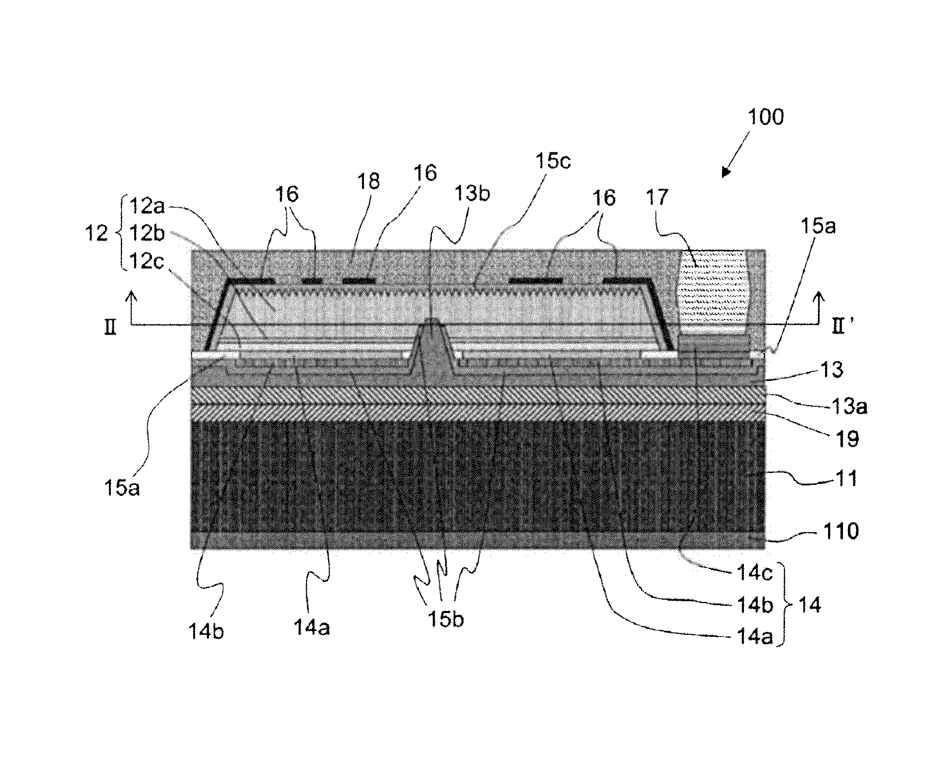
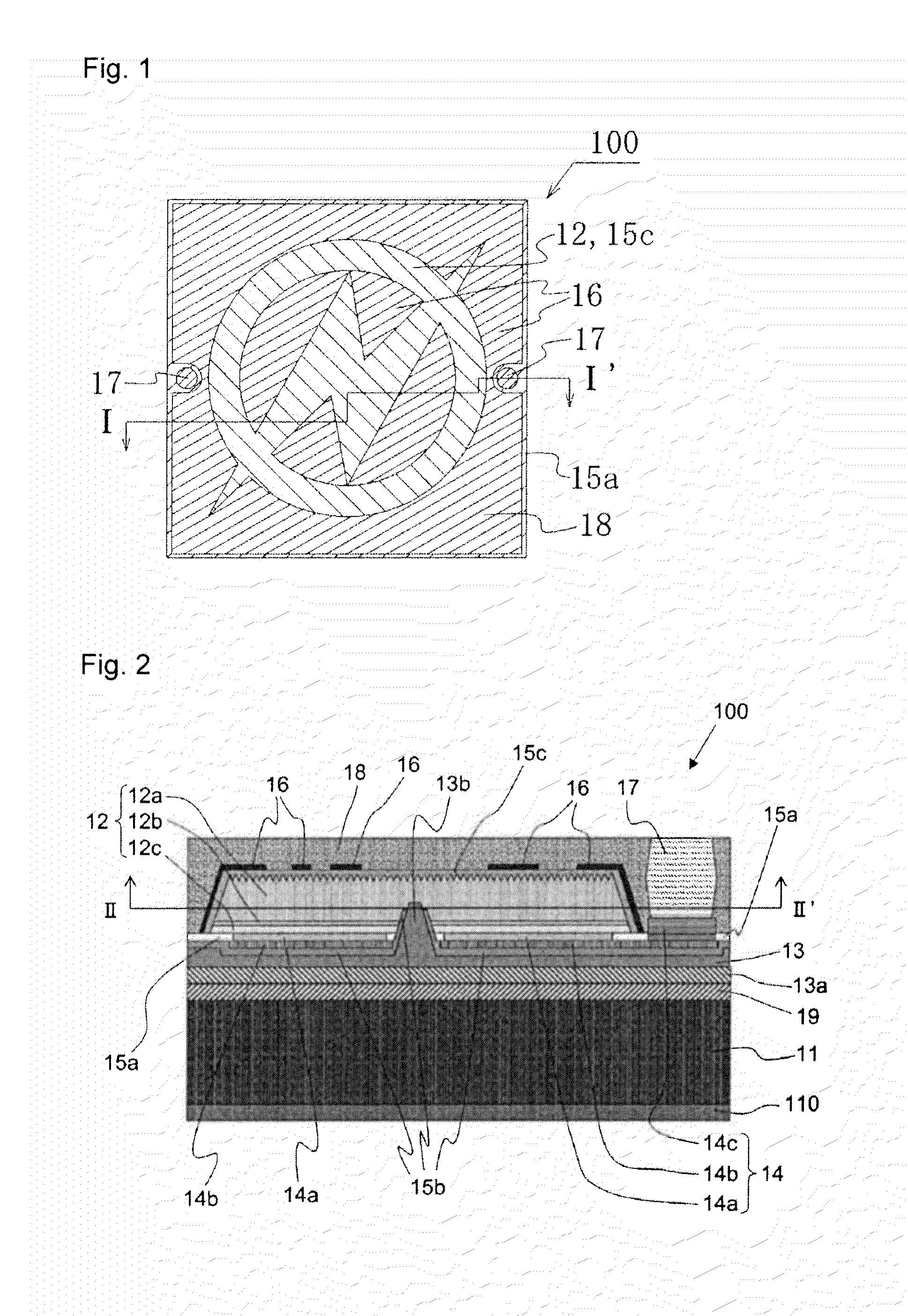
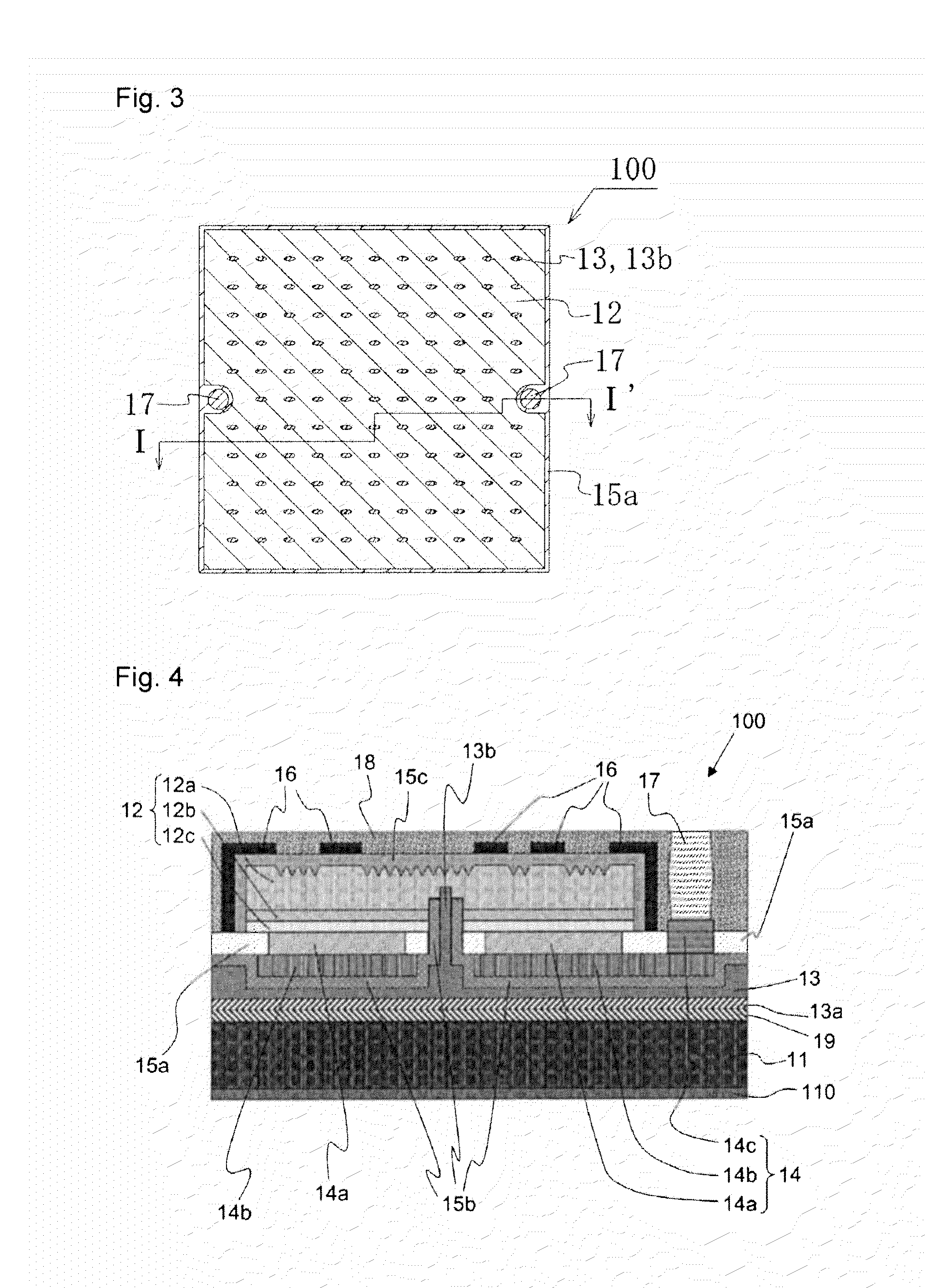
[0055]A semiconductor light emitting element according to a first embodiment is described below with reference to drawings. FIG. 1 is a schematic plane view illustrating the semiconductor light emitting element according to the first embodiment. FIG. 2 illustrates the semiconductor light emitting element according to the first embodiment, more specifically, is a schematic cross sectional view taken along line I-I′ of FIG. 1. FIG. 3 illustrates the semiconductor light emitting element according to the first embodiment, more specifically, is a schematic plane view taken along line II-II′ of FIG. 2 (a protective film 15c, a light shielding member 16, and a wavelength conversion member 18 are not illustrated). The line I-I′ of FIGS. 1 and 3 illustrates the same line. FIG. 4 is a schematic cross sectional view illustrating a modification of the semiconductor light emitting element according to the first embodiment. FIG. 5 is a schematic plane view illustrating a modification of the semic...
second embodiment
[0095]A semiconductor light emitting element according to a second embodiment is described below. FIG. 6 is a schematic plane view illustrating the semiconductor light emitting element according to the second embodiment. FIG. 7 illustrates semiconductor light emitting element according to the second embodiment and is a schematic cross sectional view taken along line of FIG. 6. FIG. 8 is a schematic cross sectional view illustrating a modification of the semiconductor light emitting element according to the second embodiment. However, for the convenience sake for description, FIGS. 6 through 8 are not equally scaled. A semiconductor light emitting element 200 according to the second embodiment is substantially the same as the first embodiment except for shapes and positions of the light shielding member 26 and the wavelength conversion member 28.
[0096]The semiconductor light emitting element 200 according to the second embodiment is provided with the light shielding member 26 coverin...
third embodiment
[0100]Now, a semiconductor light emitting element according to a third embodiment is described below. FIG. 9 is a lateral profile illustrating a shape of the reflecting electrode 34a in the semiconductor light emitting element according to the third embodiment. Here, the lateral profile is a cross sectional in parallel with the upper surface of the support substrate. A semiconductor light emitting element 300 according to the third embodiment is substantially identical to the first embodiment except that a shape of the reflecting electrode 34a differs. The lateral profile does not illustrates the semiconductor laminated structural body, the insulating film, the protective film, the light shielding member, the bump, and the wavelength conversion member which, however, are similar to those of the first embodiment.
[0101]In the semiconductor light emitting element 300 according to the third embodiment, the reflecting electrode 34a has a flat surface of a shape similar to the opening of ...
PUM
 Abstract
Description
Claims
Application Information