Method and apparatus for forming crystallized semiconductor layer, and method for manufacturing semiconductor apparatus

a technology of crystallized semiconductors and manufacturing methods, applied in semiconductor devices, instruments, optics, etc., can solve the problems of deterioration of the quality of the semiconductor film formed on the porous film, lowering the strength of the manufactured thin film semiconductor device, etc., and achieves the improvement of the mobility of electrons or holes

Inactive Publication Date: 2005-01-20
ADVANCED LCD TECH DEVMENT CENT
View PDF3 Cites 14 Cited by
  • Summary
  • Abstract
  • Description
  • Claims
  • Application Information

AI Technical Summary

Benefits of technology

[0014] It is an object of the present invention to provide a method for forming a crystallized semiconductor layer in which crystallized grain formation positions are aligned and electron or hole mobility characteristics are also unified, a method for manufacturing a semiconductor apparatus, an apparatus for forming a crystallized semiconductor layer and a method for manufacturing a display apparatus. That is, in a thin film semiconductor apparatus in which a unit electrical circuit is arranged in accordance with each crystallized grain having a large particle size, irregularities in mobility of electrons or holes are improved.

Problems solved by technology

Although providing the porous film is effective for reducing heat conduction, the strength of the manufactured thin film semiconductor device may be possibly lowered due to the brittleness derived from the porosity, and there is a problem that the quality of the semiconductor film formed on the porous film is deteriorated.

Method used


Image

  • Method and apparatus for forming crystallized semiconductor layer, and method for manufacturing semiconductor apparatus
  • Method and apparatus for forming crystallized semiconductor layer, and method for manufacturing semiconductor apparatus
  • Method and apparatus for forming crystallized semiconductor layer, and method for manufacturing semiconductor apparatus

Examples


Embodiment Construction

[0038] Embodiments according to the present invention will now be described with reference to the accompanying drawings. In respective figures, like reference numerals denote substantially the same or similar parts or members, and their detailed explanations will be eliminated.

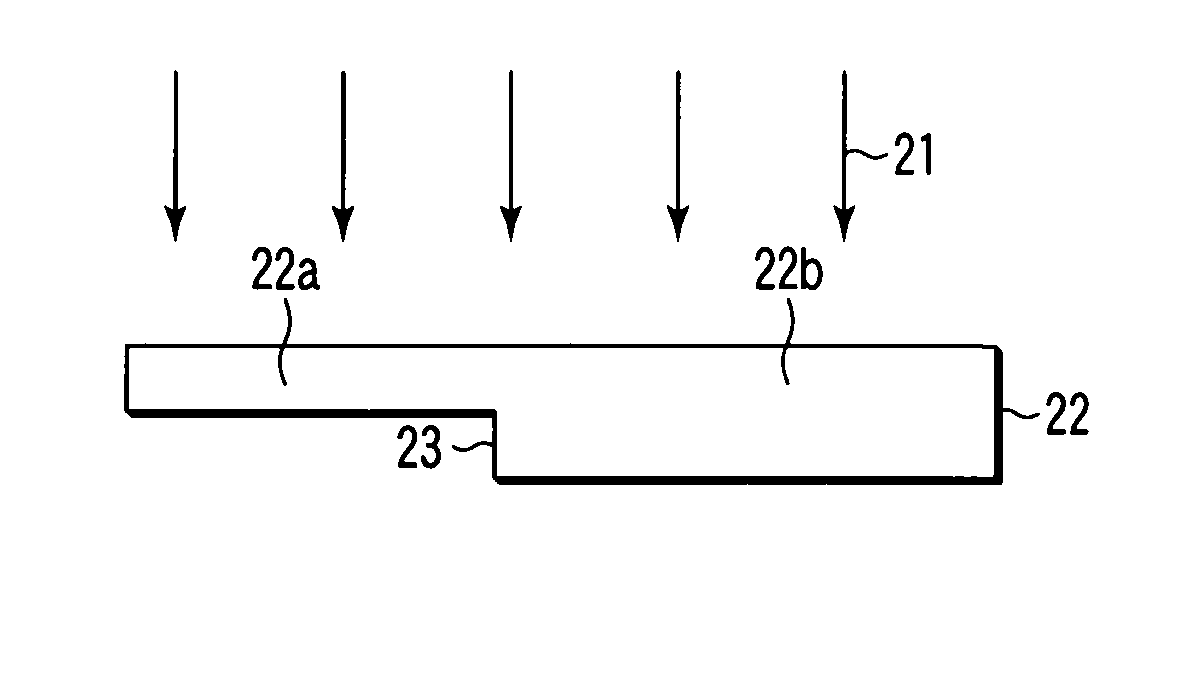
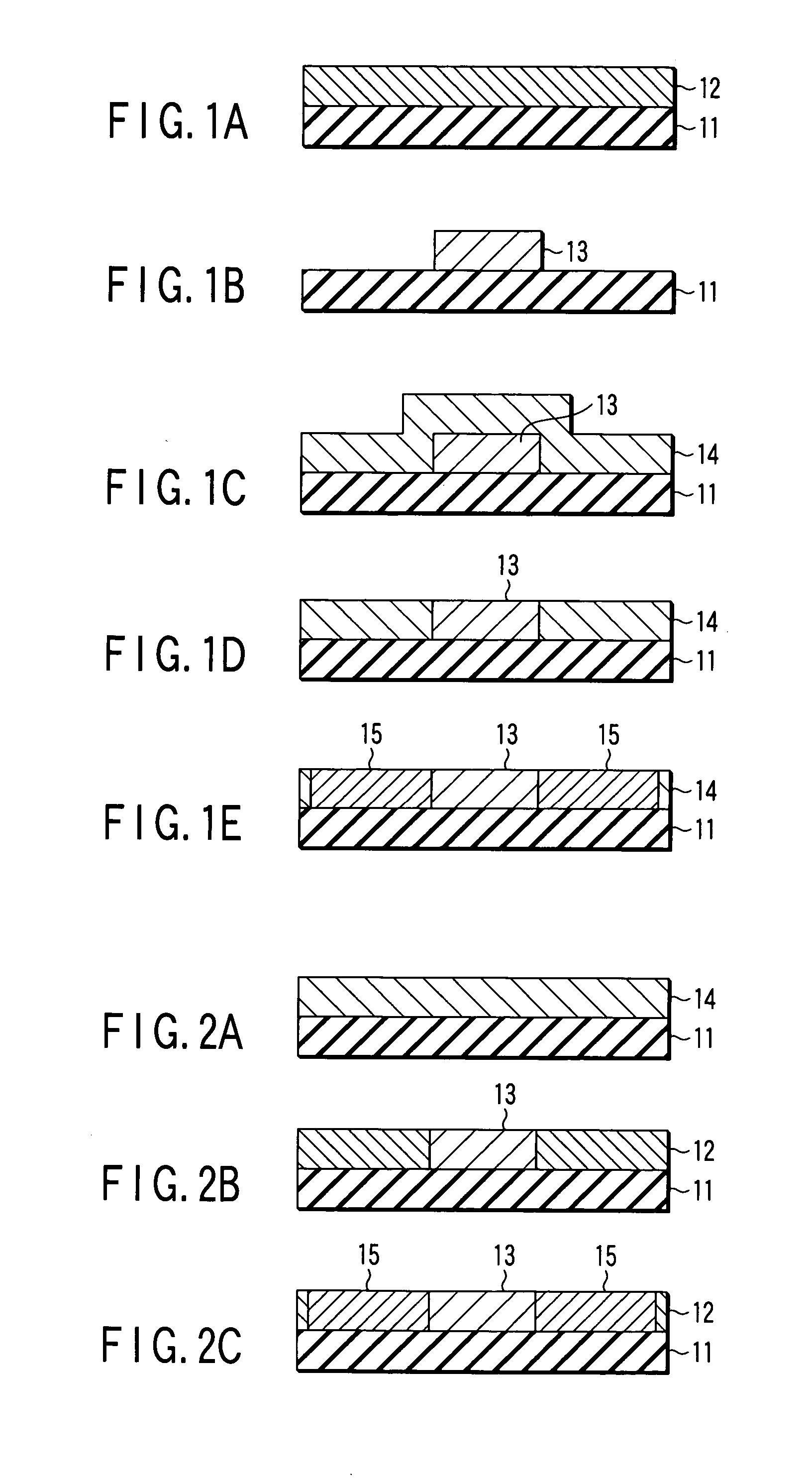
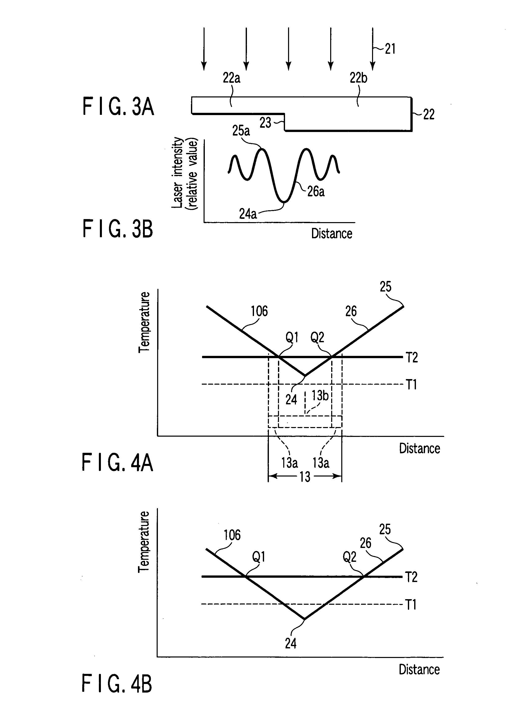
[0039] In the present invention, as arrangement conformations of a crystal seed, there are roughly two types of conformations. An example of a first conformation will now be described with reference to FIGS. 1A to 1E.

[0040] A non-single crystal semiconductor such as an amorphous silicon film 12 is formed on an insulative base substance 11 formed of a glass substrate or the like by a known film formation method, e.g., a CVD method (FIG. 1A). Thus, a base body is formed in order to form this amorphous silicon film 12 as a crystal seed, crystallization processing is applied by a known method, e.g., the method described in the section “background”, and shaping processing is applied to the film in order to obtain...


PUM

PropertyMeasurementUnit
electron mobilityaaaaaaaaaa
particle sizeaaaaaaaaaa
temperatureaaaaaaaaaa

Abstract

A method for forming a crystallized semiconductor layer includes preparing a non-single-crystal semiconductor layer in which at least one crystal seed is formed, and irradiating with an energy ray the non-single-crystal semiconductor layer having the crystal seed formed therein to allow a crystal to laterally grow from the crystal seed in the non-single-crystal semiconductor layer, irradiation of the energy ray is carried out by positioning to at least a part of the crystal seed an area having a minimum intensity value of the energy ray, the energy ray having a confirmation that an area having a maximum intensity value of the energy ray is continuously reduced to the area having the minimum intensity value in an irradiated surface.

Description

CROSS-REFERENCE TO RELATED APPLICATIONS [0001] This application is based upon and claims the benefit of priority from prior Japanese Patent Application No. 2003-158136, filed Jun. 3, 2003, the entire contents of which are incorporated herein by reference. BACKGROUND OF THE INVENTION [0002] 1. Field of the Invention [0003] The present invention relates to a method for forming a crystallized semiconductor layer which is crystallized from a non-single-crystal semiconductor layer by using laser beams, a method for manufacturing a semiconductor apparatus, an apparatus for forming a crystallized semiconductor layer, and a method for manufacturing a display apparatus. [0004] 2. Description of the Related Art [0005] As well known, a thin film semiconductor device such as a thin film transistor (TFT) has a substrate in which a semiconductor layer consisting of a semiconductor substance such as silicon is formed on a base substance consisting of an insulating material such as quartz glass. In...

Claims


Application Information

Patent Timeline
Patent Type & Authority Applications(United States)
IPC IPC(8): G02F1/1345G02F1/1368H01L21/00H01L21/02H01L21/20H01L21/268H01L21/324H01L21/335H01L21/336H01L29/78H01L29/786
CPCH01L29/66772H01L21/2026H01L21/02686H01L21/02678H01L21/02422H01L21/02532H01L21/02691
Inventor YAMAMOTO, YOSHITAKANISHITANI, MIKIHIKOHIRAMATSU, MASATOJYUMONJI, MASAYUKIKIMURA, YOSHINOBU
Owner ADVANCED LCD TECH DEVMENT CENT
Why Eureka
Try Eureka