Portable Electronic Device

a portable electronic device and electronic device technology, applied in the field of electronic devices, can solve the problems of difficult to meet the requirements of thin portable electronic devices, difficult to remove the frame of the housing, and the inability to visually hide the insulation layer and the fpc pattern of the substrate, etc., to achieve the effect of facilitating a thin type of portable electronic devices

Active Publication Date: 2013-10-31
WISTRON CORP
View PDF5 Cites 4 Cited by
  • Summary
  • Abstract
  • Description
  • Claims
  • Application Information

AI Technical Summary

Benefits of technology

[0010]Besides, another object of the present invention is to provide a novel portable electronic device and a touch control module for removing the thickness issue induced by the necessity of the double substrates or the cover lens through the design of the substrate structure.
[0024]Furthermore, by using the touch control module of the present invention, only a single substrate is required, which removes the requirements of double substrates or transparent bonding or cover lens and facilitates a thin type of the portable electronic device.

Problems solved by technology

The substrate is made of transparent materials, e.g. glass, but bonding materials formed on a border of the substrate are translucent or colored, such that the substrate may not visually hide the insulation layer and the FPC pattern when the user looks at the touch panel from a side view.
As a result, the housing is hard to get rid of the frame.
More importantly, the touch panel of the conventional portable electronic devices is composed by two substrates, which is hard to comply with the requirement of thin portable electronic devices.
Moreover, the touch panel may include a cover lens to protect the inner circuits and elements, which further increases the thickness of the touch panel as well as the thickness of the portable electronic device.

Method used


Image

  • Portable Electronic Device
  • Portable Electronic Device
  • Portable Electronic Device

Examples


Embodiment Construction

[0030]Descriptions below refer the related figures to illustrate a portable electronic device according to a preferred embodiment of the present invention, wherein the identical elements are illustrated by the same symbols.

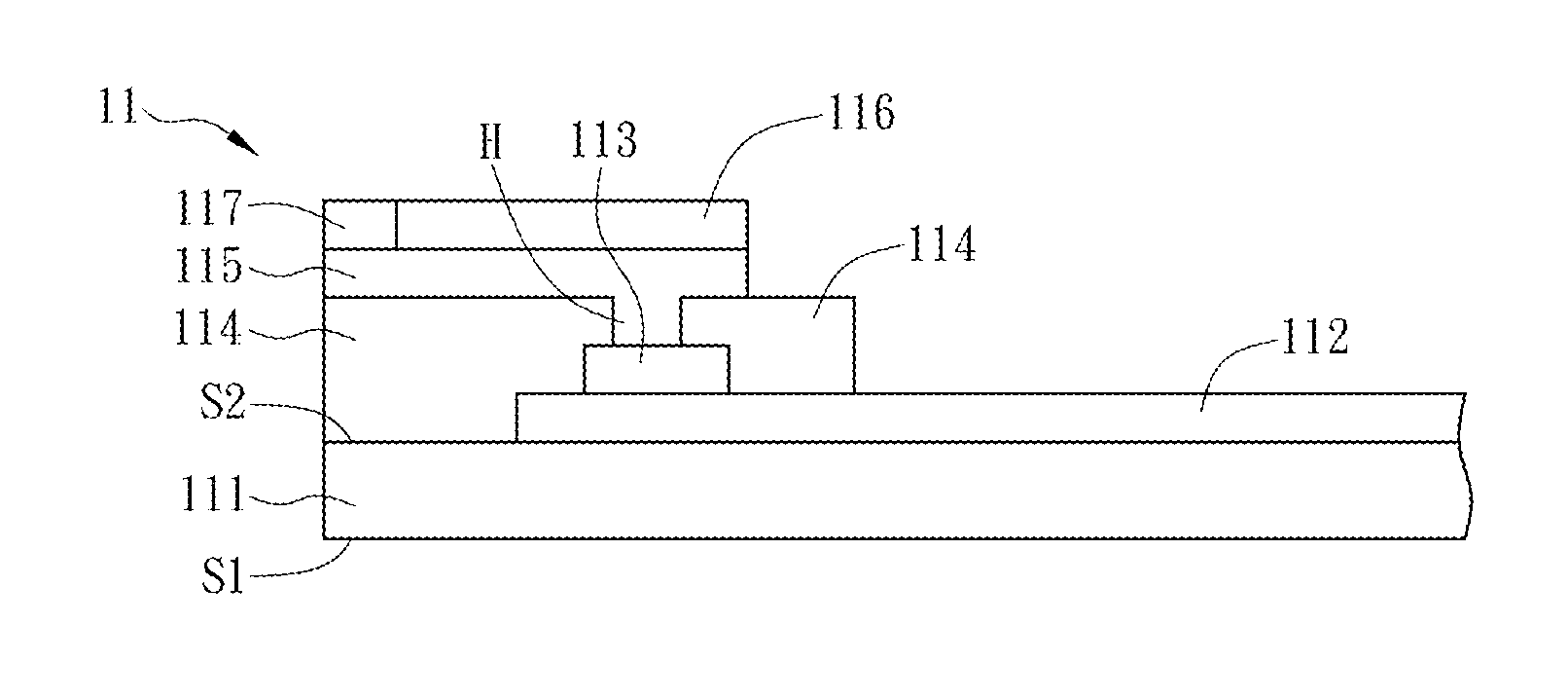
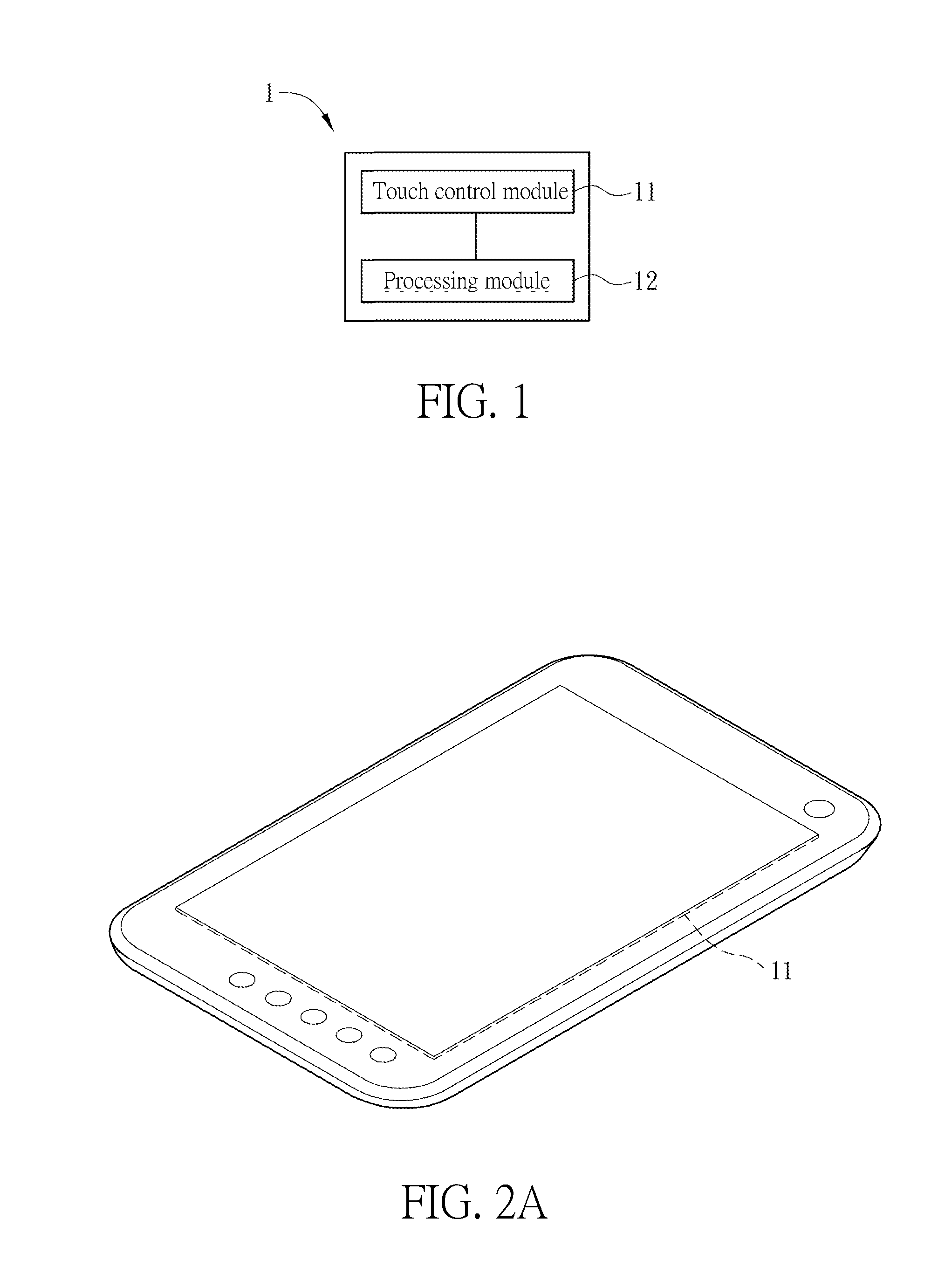
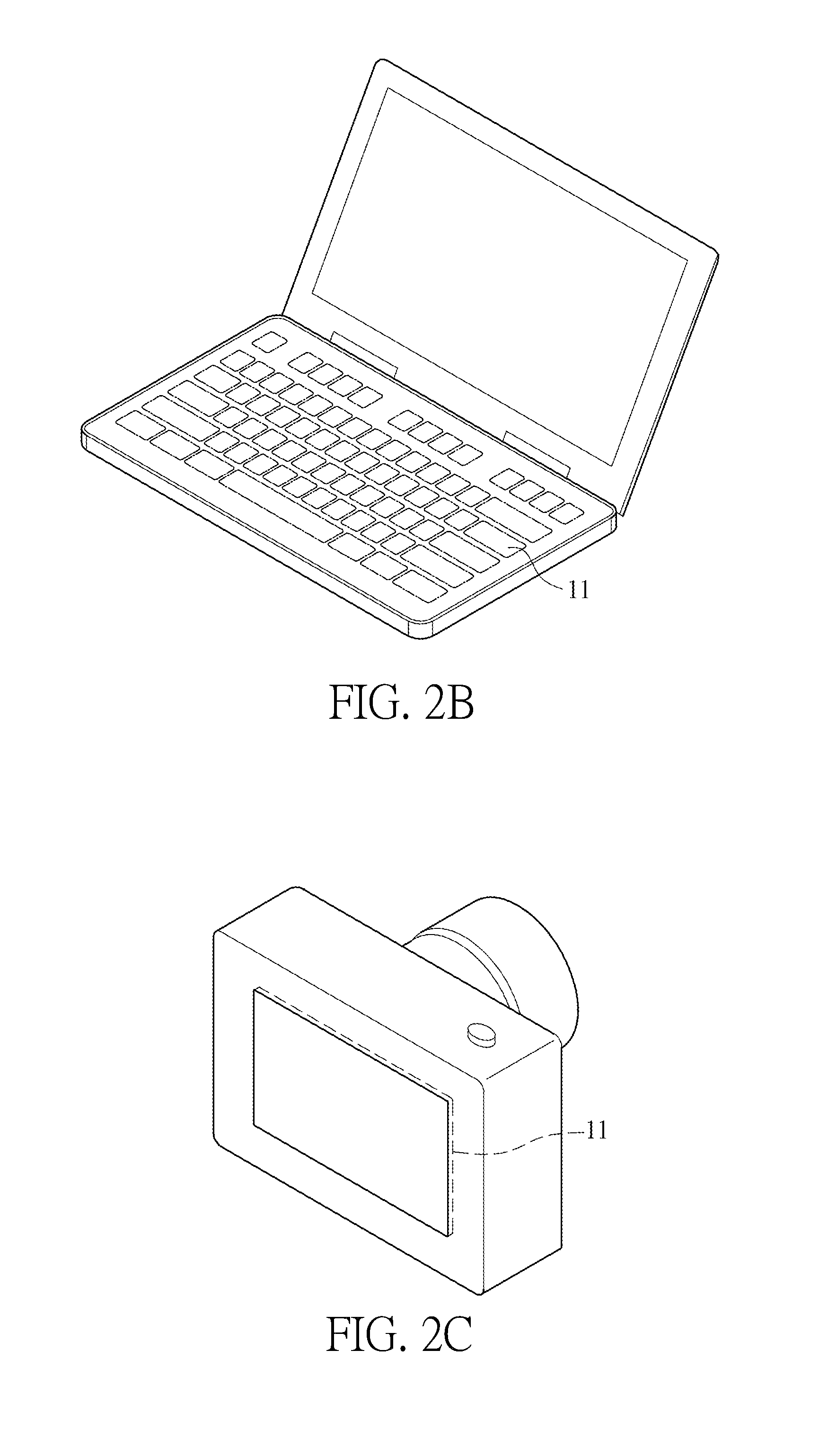
[0031]Please refer to FIG. 1, which is a block diagram of a portable electronic device 1 according to an embodiment of the present invention. The portable electronic device 1 includes a touch control module 11 and a processing module 12. The touch control module 11 and the processing module 12 are electrically connected. In the embodiment, the portable electronic device 1 may be a tablet PC, a laptop, a digital camera, an audio and video playback device, a game console or a mobile communication device, as shown in FIG. 2A to FIG. 2F. Besides, the portable electronic device 1 may also be a touch keyboard, wherein the touch control module 11 thereof is printed or disposed by a physical pattern in an operation side to visually form into multiple keys. The keys may ac...


PUM


Abstract

A portable electronic device includes a touch control module and a processing module. The touch control module has a substrate, a transparent conductive layer, a conductive decoration pad, a decoration layer and a non-transparent conductive layer. The transparent conductive layer is disposed on the substrate. The conductive decoration pad is disposed on the transparent conductive layer. The decoration layer is disposed on the conductive decoration pad and the transparent conductive layer, and has an opening. The non-transparent conductive layer is disposed on the decoration layer and electrically connected with the transparent conductive layer via the opening. The processing module is electrically connected with the touch control module.

Description

BACKGROUND OF THE INVENTION[0001]1. Field of the Invention[0002]The present invention relates to an electronic device, and more particularly, to a portable electronic device.[0003]2. Description of the Prior Art[0004]Various types of touch input technology are widely used in electronic products, especially portable electronic devices, e.g. mobile phones and tablet PCs. A portable electronic device uses a touch panel as an input interface, such that a user may perform touch operations on the touch panel to input commands, e.g. drag a finger to move a cursor or write words on the touch panel. Also, the touch panel may cooperate with a display to show virtual keys for being selected by the user to input characters and words.[0005]In general, touch panels are categorized into resistive, capacitive, ultrasound, and infrared types, wherein the resistive touch panels are the most popular. The resistive touch panels may be further categorized into 4-wire, 5-wire, 6-wire, and 8-wire touch pa...

Claims


Application Information

Patent Timeline
Patent Type & Authority Applications(United States)
IPC IPC(8): G06F3/044
CPCG06F3/044G06F1/1626G06F1/1637G06F1/1643G06F3/041
Inventor WANG, KUEI-CHINGLIN, TA-HULIU, TUNG-HSIN
Owner WISTRON CORP
Why Eureka
Try Eureka