Electronic component

a technology of electronic components and components, applied in the field of electronic components, can solve the problems of increasing the stress of the solder due to temperature changes, the and the increase of the temperature of the solder, so as to prevent the formation of a crack in the solder during us

Active Publication Date: 2013-11-07
MURATA MFG CO LTD
View PDF8 Cites 18 Cited by
  • Summary
  • Abstract
  • Description
  • Claims
  • Application Information

AI Technical Summary

Benefits of technology

[0011]Various preferred embodiments of the present invention prevent inclination of the electronic component relative to the circuit board when the electronic component is mounted, and further prevent formation of a crack in a solder during use.

Problems solved by technology

However, in the monolithic ceramic capacitor 500 described in Japanese Unexamined Utility Model Registration Application Publication No. 62-135427, it is difficult to not only prevent inclination of the monolithic ceramic capacitor 500 relative to the circuit board when the monolithic ceramic capacitor 500 is mounted, but also to prevent formation of a crack in the solder during use.
However, when the height of each fillet in the z-axis direction increases, stress caused in the solder due to changes in temperature also increase.
As a result, there is a risk that a crack may occur in the fillet during use.
Thus, as described above, it is difficult to keep preventing inclination of the monolithic ceramic capacitor 500 relative to the circuit board when the monolithic ceramic capacitor 500 is mounted while preventing formation of the crack in the solder during use.

Method used


Image

  • Electronic component
  • Electronic component
  • Electronic component

Examples


Embodiment Construction

[0019]An electronic component according to a preferred embodiment of the present invention will be described below with reference to the drawings.

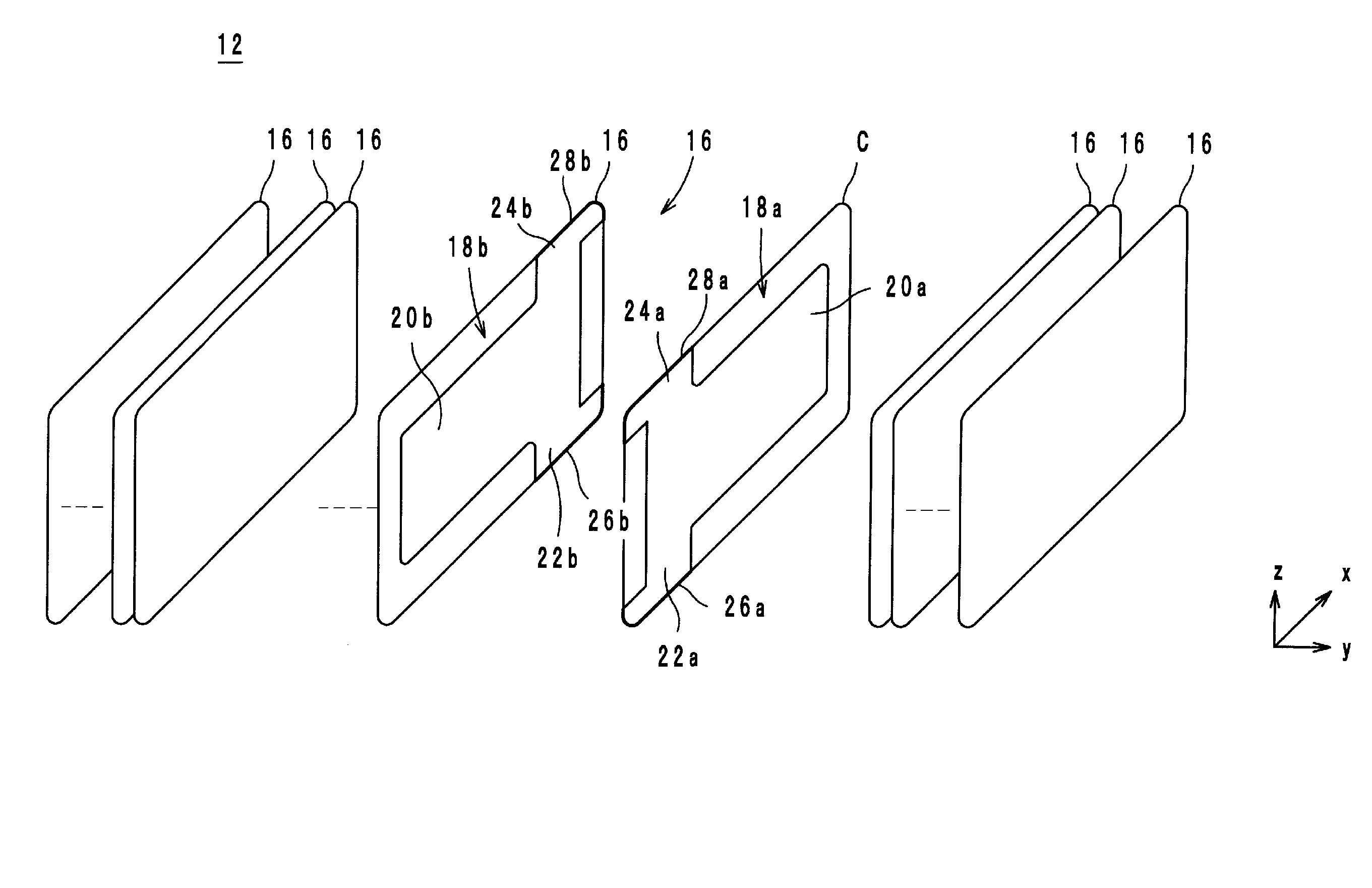
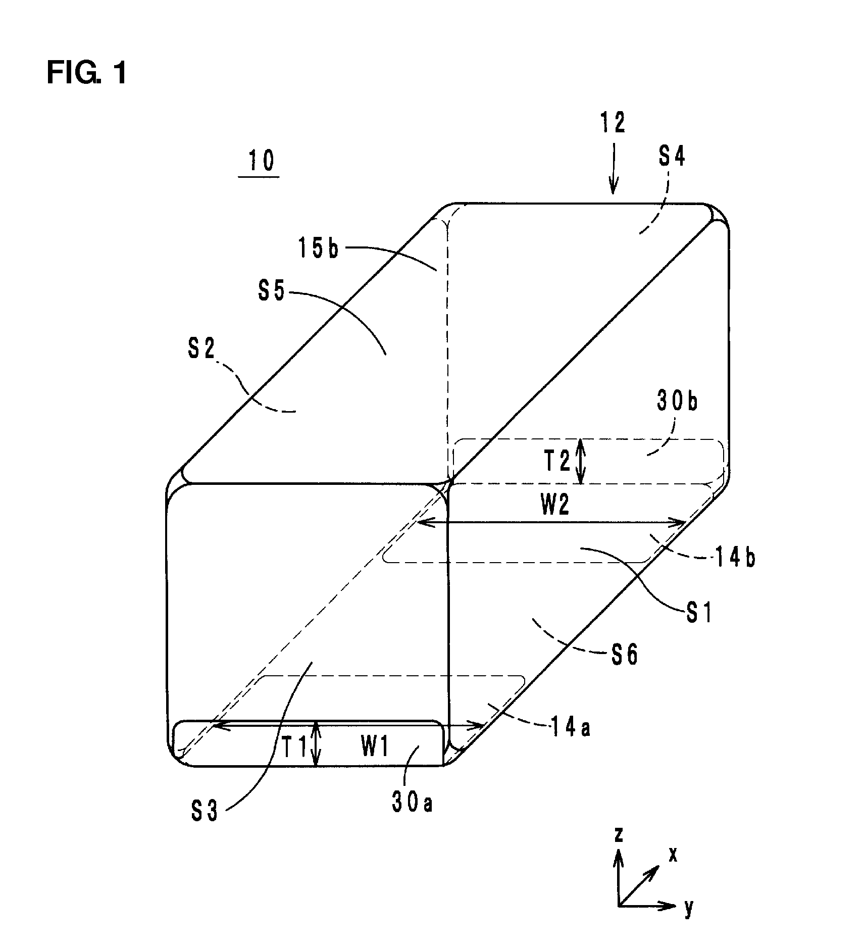
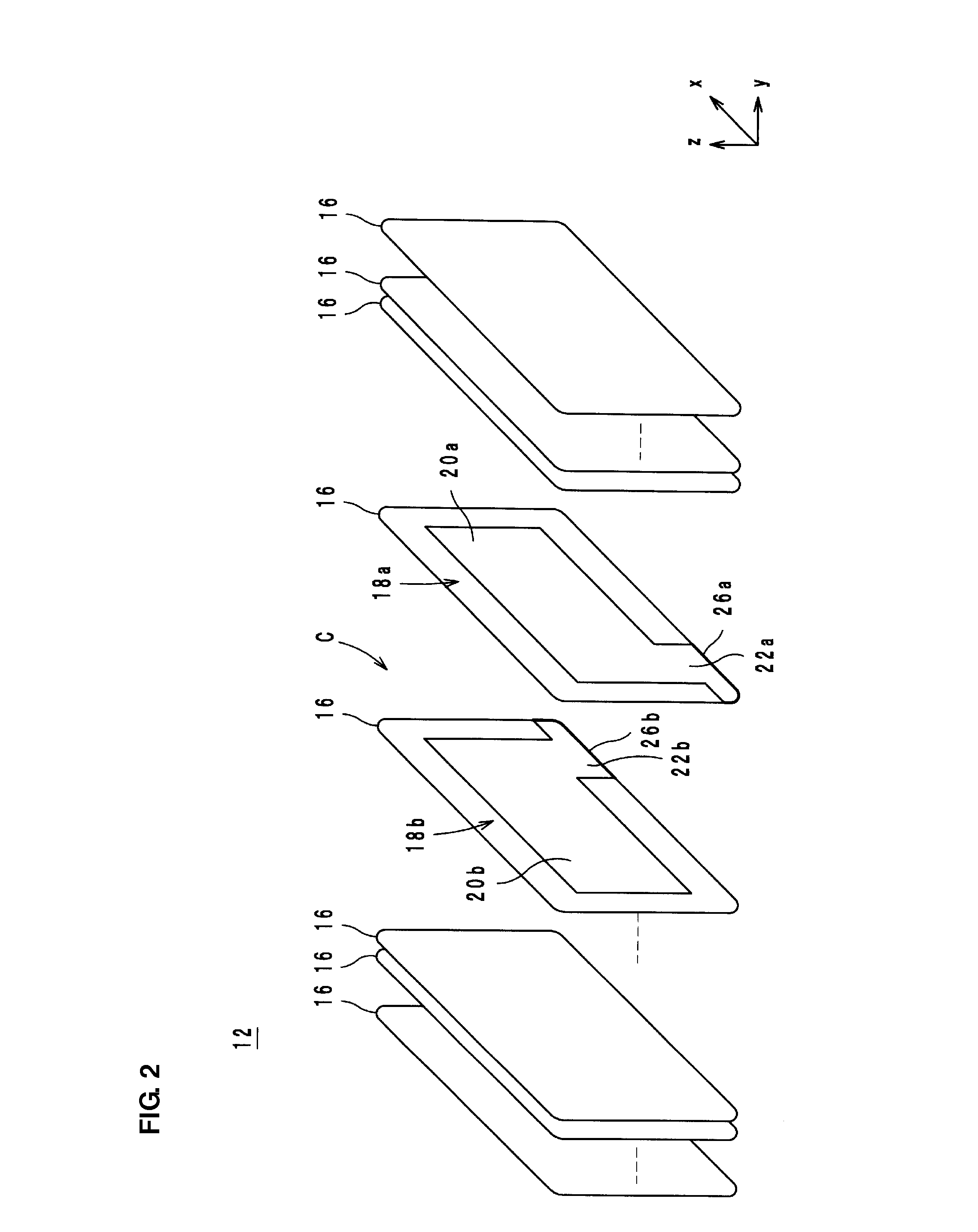
[0020]First, the construction of the electronic component is described with reference to the drawings. FIG. 1 is an external perspective view of an electronic component according to the present preferred embodiment of the present invention. FIG. 2 is an exploded perspective view of a laminate 12 in the electronic component 10 of FIG. 1. In the following, a laminating direction of the laminate 12 is defined as a y-axis direction. When viewing the laminate 12 in a plan view in the y-axis direction, a direction of a long side of the laminate 12 is defined as an x-axis direction. When viewing the laminate 12 in a plan view in the y-axis direction, a direction of a short side of the laminate 12 is defined as a z-axis direction.

[0021]The electronic component 10 is preferably a chip capacitor, for example. As illustrated in FIGS. 1 and 2, the ele...


PUM

PropertyMeasurementUnit
thicknessaaaaaaaaaa
thicknessaaaaaaaaaa
thicknessaaaaaaaaaa

Abstract

In an electronic component, a body includes top and bottom surfaces, first and second end surfaces, and first and second lateral surfaces. A first outer electrode partially extends over the bottom surface and the first end surface without being disposed on the top surface, the second end surface, and both the lateral surfaces. A second outer electrode partially extends over the bottom surface and the second end surface without being disposed on the top surface, the first end surface, and both the lateral surfaces. An area of a first end surface portion of the first outer electrode disposed on the first end surface and area of a second end surface portion of the second outer electrode disposed on the second end surface are in a range of about 6.6% to about 35.0% of area of the first and second end surfaces, respectively.

Description

BACKGROUND OF THE INVENTION[0001]1. Field of the Invention[0002]The present invention relates to an electronic component, and more particularly, to a chip-type electronic component mounted on a circuit board.[0003]2. Description of the Related Art[0004]As a related art electronic component, for example, a chip-type monolithic ceramic capacitor is described in Japanese Unexamined Utility Model Registration Application Publication No. 62-135427. FIG. 6 is a perspective view of the chip-type monolithic ceramic capacitor (hereinafter referred to simply as the “monolithic ceramic capacitor”) 500 described in Japanese Unexamined Utility Model Registration Application Publication No. 62-135427. In FIG. 6, a laminating direction is defined as a y-axis direction. When looking at the monolithic ceramic capacitor 500 in a plan view from the y-axis direction, a direction in which a short side of the monolithic ceramic capacitor 500 extends is defined as a z-axis direction, and a direction in wh...

Claims


Application Information

Patent Timeline
Patent Type & Authority Applications(United States)
IPC IPC(8): H01G4/008
CPCH01G4/008H01G4/0085H01G4/012H01G4/12H01G4/1218H01G4/232H01G4/30
Inventor TAKEUCHI, SYUNSUKEOTA, YUTAKA
Owner MURATA MFG CO LTD
Why Eureka
Try Eureka