Etch resistant barrier for replacement gate integration

a technology of replacement gate and barrier, which is applied in the field of barrier employed in the fabrication of semiconductor devices, can solve the problems of difficult scheme and poor wet etch resistance of oxid

Inactive Publication Date: 2013-11-21
IBM CORP
View PDF15 Cites 67 Cited by
  • Summary
  • Abstract
  • Description
  • Claims
  • Application Information

AI Technical Summary

Problems solved by technology

Integration of complementary metal-oxide-semiconductor (CMOS) devices at the 22 nm node and beyond presents several important challenges.
Although the oxide is relatively easy to apply in this way, the oxide has a very poor wet etch resistance due to the restricted thermal budget it imposes.
This scheme can be challenging due to the high aspect ratios of high-k metal gates (HKMGs) in finFET and Trigate device geometries.

Method used


Image

  • Etch resistant barrier for replacement gate integration
  • Etch resistant barrier for replacement gate integration
  • Etch resistant barrier for replacement gate integration

Examples


Embodiment Construction

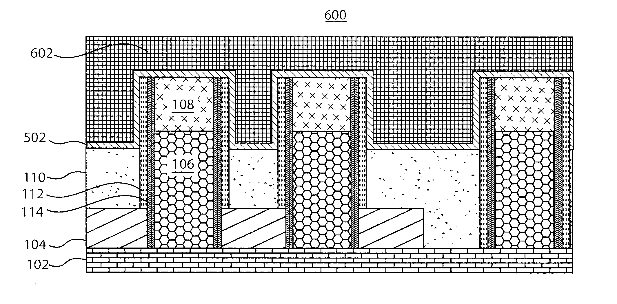
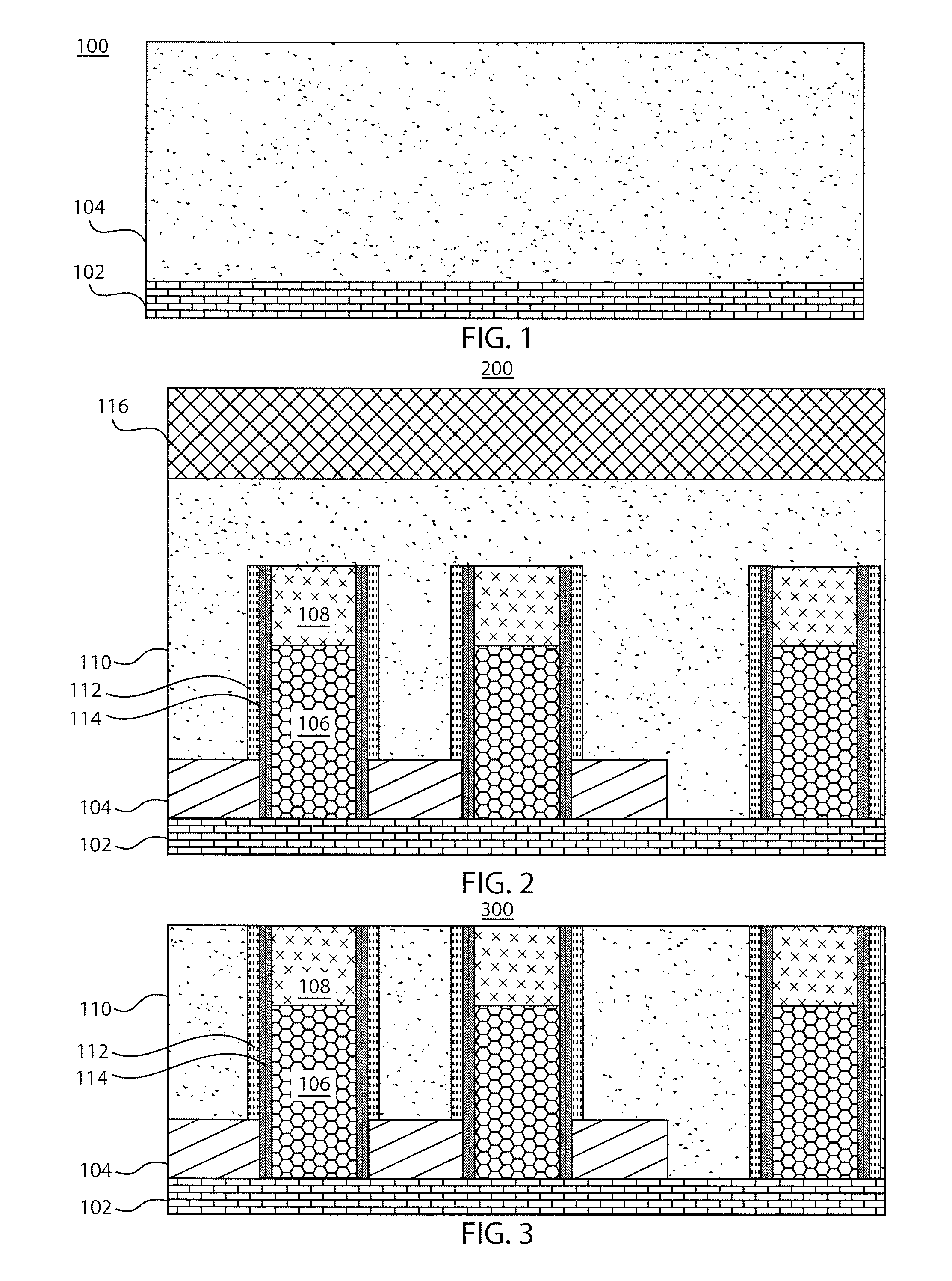
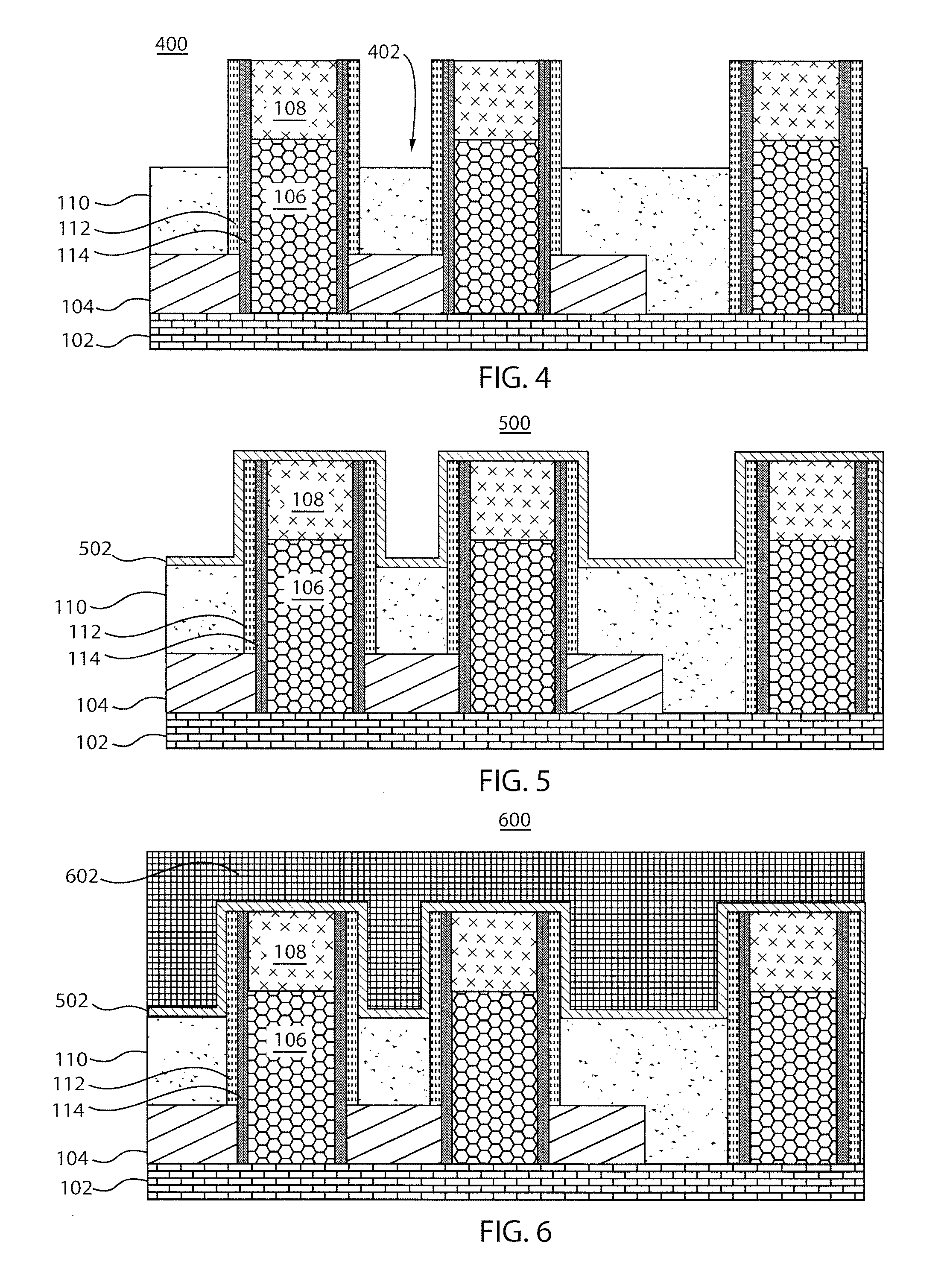
[0029]Embodiments of the present principles are directed to facilitating the fabrication of CMOS devices. For example, the embodiments described herein provide substantial advantages and benefits for replacement metal gate fabrication schemes. As noted above, if RMG schemes are employed to fabricate small scale devices, a gap filling layer that has a high aspect ratio and exhibits wet etch resistance properties as well ease of application should be applied between the gates prior to performing contact etching.

[0030]As also noted above, one method of fabricating CMOS devices caps the gap fill oxide with an HDP process. However, this approach has several disadvantages. For example, the aspect ratio of the gap fill layer is limited to 4:1, beyond which it is increasingly difficult to maintain a gap fill material that is free of defects using HDP. Even at the 4:1 aspect ratio, the gap filling process requires a large number deposition and etch cycles when HDP is employed. The large numb...


PUM


Abstract

Semiconductor devices and methods of their fabrication are disclosed. One method includes forming a semiconductor device structure including a plurality of dummy gates and a dielectric gap filling material with a pre-determined aspect ratio that is between the dummy gates. An etch resistant nitride layer is applied above the dielectric gap filling material to maintain the aspect ratio of the gap filling material. In addition, the dummy gates are removed by implementing an etching process. Further, replacement gates are formed in regions of the device structure previously occupied by the dummy gates.

Description

BACKGROUND[0001]1. Technical Field[0002]The present invention relates to semiconductor devices, and more particularly to barriers employed in the fabrication of semiconductor devices.[0003]2. Description of the Related Art[0004]Integration of complementary metal-oxide-semiconductor (CMOS) devices at the 22 nm node and beyond presents several important challenges. For example, due to the small scale of the devices and the three-dimensional configuration of finFET and Trigate devices, a high aspect ratio gap filling layer should be applied between the gates during fabrication prior to performing contact etching. With regard to replacement metal gate schemes in particular, in addition to providing a defect-free gap fill and a relative ease of application, this gap filling layer should exhibit very good wet etch resistance properties.[0005]During fabrication of a CMOS device, a gap filling layer can be formed by implementing spin-on glass (SOG) techniques or Chemical Vapor Deposition (C...

Claims


Application Information

Patent Timeline
Patent Type & Authority Applications(United States)
IPC IPC(8): H01L21/28
CPCH01L21/845H01L27/1211H01L29/66545H01L29/785
Inventor JAGANNATHAN, HEMANTHMEHTA, SANJAYYEH, CHUN-CHEN
Owner IBM CORP
Why Eureka
Try Eureka