Solid-state imaging element, method of driving solid-state imaging element, and imaging device

Inactive Publication Date: 2013-11-28
FUJIFILM CORP
View PDF2 Cites 19 Cited by
  • Summary
  • Abstract
  • Description
  • Claims
  • Application Information

AI Technical Summary

Benefits of technology

[0029]According to the present invention, it is possible to provide a photoelectric converting layer-stacked solid-state imaging element, and a method

Problems solved by technology

Such an image lag over the plurality of frames causes serious deterior

Method used


Image

  • Solid-state imaging element, method of driving solid-state imaging element, and imaging device
  • Solid-state imaging element, method of driving solid-state imaging element, and imaging device
  • Solid-state imaging element, method of driving solid-state imaging element, and imaging device

Examples


Example

[0045]Hereinafter, an embodiment of the present invention will be described with reference to the drawings.

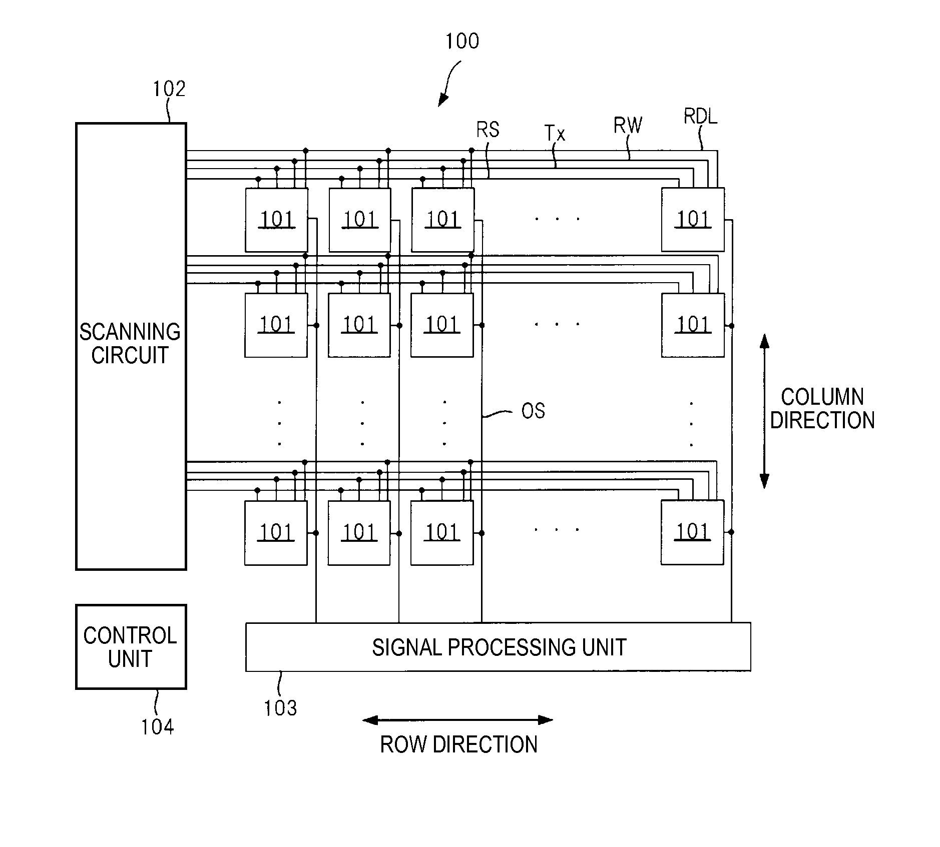
[0046]FIG. 1 is a schematic plan diagram of a photoelectric converting layer-stacked solid-state imaging element 100 for describing an embodiment of the present invention. This solid-state imaging element 100 is used by being mounted in imaging devices such as digital cameras, and digital video cameras, imaging modules mounted in electronic endoscopes, and mobile telephones with camera, and the like.

[0047]The solid-state imaging element 100 shown in FIG. 1 includes a plurality of pixels 101 arrayed in a two-dimensional shape (a square grid shape in the example of FIG. 1) in a row direction and a column direction orthogonal thereto, a scanning circuit 102 for controlling reading of signals output from the pixels 101, a signal processing unit 103 that processes signals output from each of the pixels 101, and a control unit 104 that controls the overall solid-state imaging element...


PUM


Abstract

A solid-state imaging element 100 includes a control unit 104 that performs, in each frame, driving to inject electric charge into a storage unit 11 from a power source supplying reset voltage by controlling the reset voltage supplied to a reset Tr 31 and to discharge some of the electric charge that has been injected into the storage unit 11 to the power source by controlling the reset voltage.

Description

CROSS REFERENCE TO RELATED APPLICATION[0001]This is a continuation of International Application No. PCT / JP2011 / 076324 filed on Nov. 15, 2011, and claims priority from Japanese Patent Application No. 2011-010282, filed on Jan. 20, 2011, the entire disclosures of which are incorporated herein by reference.TECHNICAL FIELD[0002]The present invention relates to a solid-state imaging element, a method of driving the solid-state imaging element, and an imaging device.RELATED ART[0003]A photoelectric converting layer-stacked solid-state imaging element, in which photoelectric converting elements that include a pair of electrodes and photoelectric converting layers interposed by the electrodes are provided on a silicon substrate, and which causes electric charge generated in the photoelectric converting layers to move to the silicon substrate from either of the pair of electrodes to read out signals according to the electric charge so as to be output to the outside using an MOS (Metal Oxide ...

Claims


Application Information

Patent Timeline
IPC IPC(8): H04N5/378
CPCH04N5/378H04N25/709H04N25/76H04N25/75
Inventor GOTO, TAKASHI
Owner FUJIFILM CORP
Why Eureka
Try Eureka