Oxide Thin Film Transistor, Method for Fabricating TFT, Array Substrate for Display Device and Method for Fabricating the Same

a thin film transistor and oxide technology, applied in the field of thin film transistors, can solve the problems of large number of processes, failure to maintain initial performance, and the mobility of 0.5 cmsup>2/sup>/vs of a-si tft, and achieve the effects of reducing fabrication costs, enhancing element uniformity characteristics, and preventing misalignment in the fabrication of semiconductor elements

Active Publication Date: 2013-11-28
LG DISPLAY CO LTD
View PDF6 Cites 37 Cited by
  • Summary
  • Abstract
  • Description
  • Claims
  • Application Information

AI Technical Summary

Benefits of technology

[0030]An aspect of the present invention provides an oxide thin film transistor (TFT) capable of enhancing element uniformity characteristics by preventing misalignment in fabricating a semiconductor element, and reducing fabrication cost by reducing the number of masks, a method for fabricating the same, an array substrate for a display device having the same, and a method for fabricating the same.

Problems solved by technology

However, as displays tend to have a large size and high picture quality, high device performance is required, and thus, it is determined that an existing a-Si TFT having mobility of 0.5 cm2 / Vs has reached a limitation.
Also, a-Si TFT has a problem of reliability in that as it continues to operate, device characteristics continue to be degraded to result in a failure of maintaining initial performance.
However, a fabrication of a poly-Si TFT requires a large number of processes in comparison to the a-Si TFT and investment in additional equipment should be made first.
Thus, p-Si TFT may be appropriately applied to make a display have high picture quality or applied to a product such as an OLED, or the like, but it is inferior to the existing a-Si TFT in terms of cost, so an application thereof is limited.
In particular, in the case of a p-Si TFT, due to a technical issue such as a limitation in fabrication equipment or a defect in uniformity, a fabrication process using a large substrate having a size of lm has not been realized so far, so the difficulty of the p-Si TFT in its application to a TV product is a factor making it difficult for high performance p-Si TFT to be easily settled down in the market.
In addition, in the oxide TFT according to the related art, since the process of forming the etch stop layer 19 and the process of forming the source electrode 21 and the drain electrode 23 are performed in different masking processes, the number of masking processes is increased to increase fabrication costs.

Method used


Image

  • Oxide Thin Film Transistor, Method for Fabricating TFT, Array Substrate for Display Device and Method for Fabricating the Same
  • Oxide Thin Film Transistor, Method for Fabricating TFT, Array Substrate for Display Device and Method for Fabricating the Same
  • Oxide Thin Film Transistor, Method for Fabricating TFT, Array Substrate for Display Device and Method for Fabricating the Same

Examples


Embodiment Construction

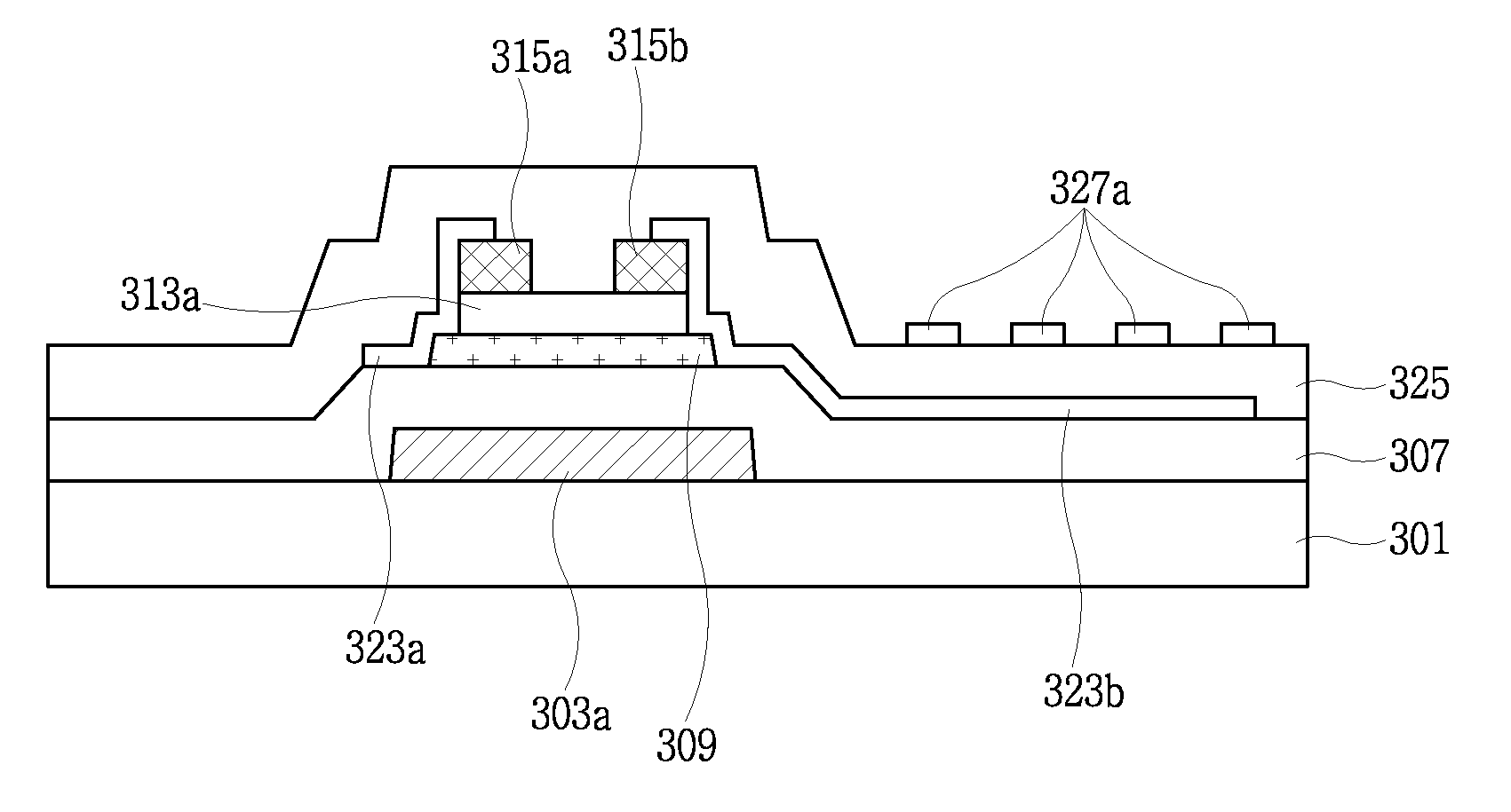
[0053]An oxide thin film transistor (TFT) structure according to embodiments of the present invention will be described in detail with reference to the accompanying drawings.

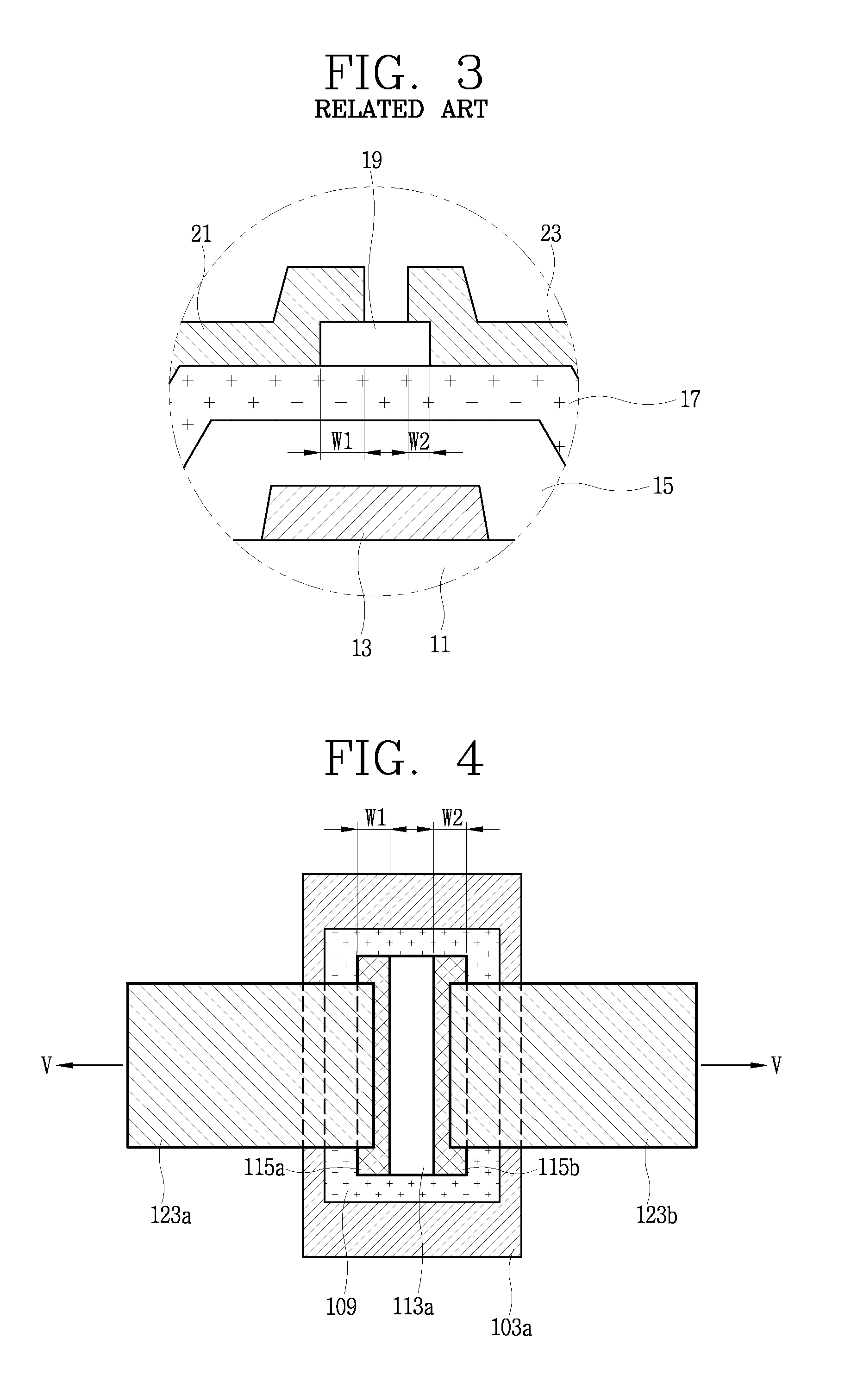
[0054]FIG. 4 is a plan view of an oxide TFT structure according to an embodiment of the present invention.

[0055]FIG. 5 is a schematic sectional view of the oxide TFT according to an embodiment of the present invention, taken along line V-V in FIG. 4.

[0056]As illustrated in FIGS. 4 and 5, an oxide TFT 100 according to an embodiment of the present invention includes a gate electrode 103a formed on a substrate 101; a gate insulating layer 107 formed on the entire surface of the substrate 101 including the gate electrode 103a; an active layer 109 formed on the gate insulating layer 107 above the gate electrode 103a; an etch stop layer pattern 113a formed on the active layer 109; a source alignment element 115a and a drain alignment element 115b formed on the etch stop layer pattern 113a and spaced apart from one ano...


PUM


Abstract

A thin film transistor (TFT), a method for fabricating a TFT, an array substrate for a display device having a TFT, and a method for fabricating the same are provided. An oxide thin film transistor (TFT) includes: a gate electrode formed on a substrate; a gate insulating layer formed on the gate electrode; an active layer formed on the gate insulating layer above the gate electrode; an etch stop layer pattern formed on the active layer; a source alignment element and a drain alignment element formed on the etch stop layer pattern and spaced apart from one another; and a source electrode in contact with the source alignment element and the active layer and a drain electrode in contact with the drain alignment element and the active layer.

Description

CROSS-REFERENCE TO RELATED APPLICATIONS[0001]The present disclosure relates to subject matter contained in priority Korean Application No. 10-2012-0055683, filed on May 24, 2012, which is herein expressly incorporated by reference in its entirety.BACKGROUND[0002]1. Field of the Invention[0003]The present invention relates to a thin film transistor (TFT) and, more particularly, to a TFT, a method for fabricating a TFT, an array substrate for a display device having a TFT, and a method for fabricating the same.[0004]2. Description of the Related Art[0005]Television products are the major application targets in the remarkably growing flat panel display market. Currently, a liquid crystal display (LCD) is a mainstream as a TV panel, and research into an application of an organic light emitting display device to TVs has been actively ongoing.[0006]Current TV display techniques are focused on major items required in the market, and the requirements in the market include a large-scale TV o...

Claims


Application Information

Patent Timeline
Patent Type & Authority Applications(United States)
IPC IPC(8): H01L29/786H01L27/15H01L29/66
CPCH01L29/7869H01L29/66969H01L27/153
Inventor YU, SANGHEE
Owner LG DISPLAY CO LTD
Why Eureka
Try Eureka