

Three-dimensional resistive random access memory devices, methods of operating the same, and methods of fabricating the same
a random access memory and three-dimensional resistive technology, applied in the field of three-dimensional resistive random access memory devices, can solve the problems of increasing the number of data bits which can be stored in a single memory cell, increasing the fabrication cost of fine-pattern technologies, etc., and achieves the effect of increasing reducing the electrical resistance of the variable resistive layer
- Summary
- Abstract
- Description
- Claims
- Application Information
AI Technical Summary
Benefits of technology
Problems solved by technology
Method used
Image

Examples
first embodiment
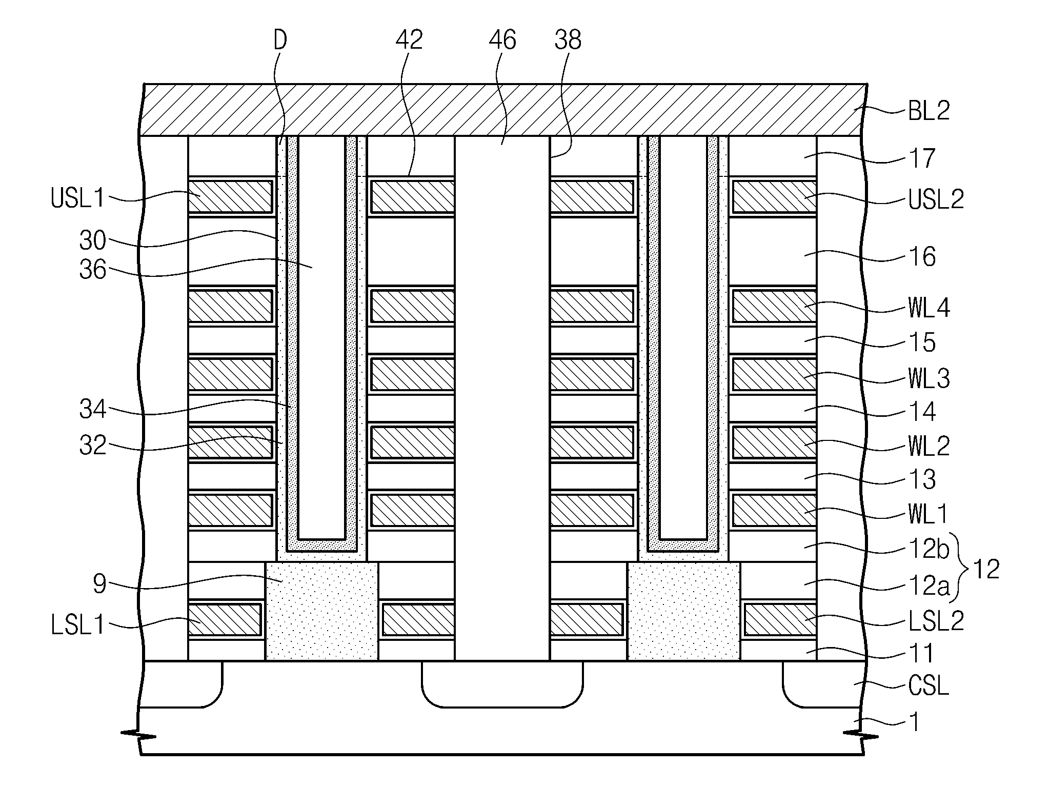
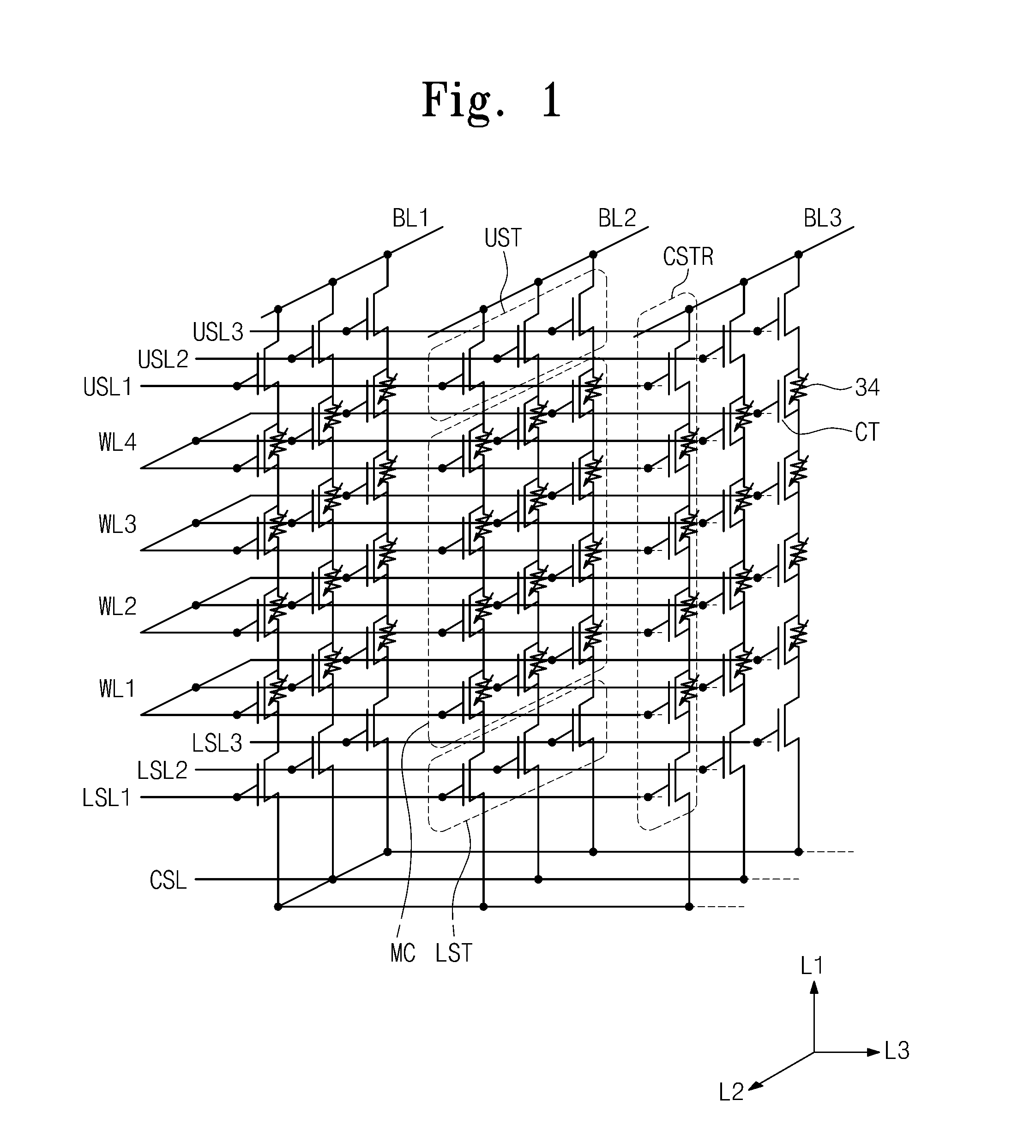
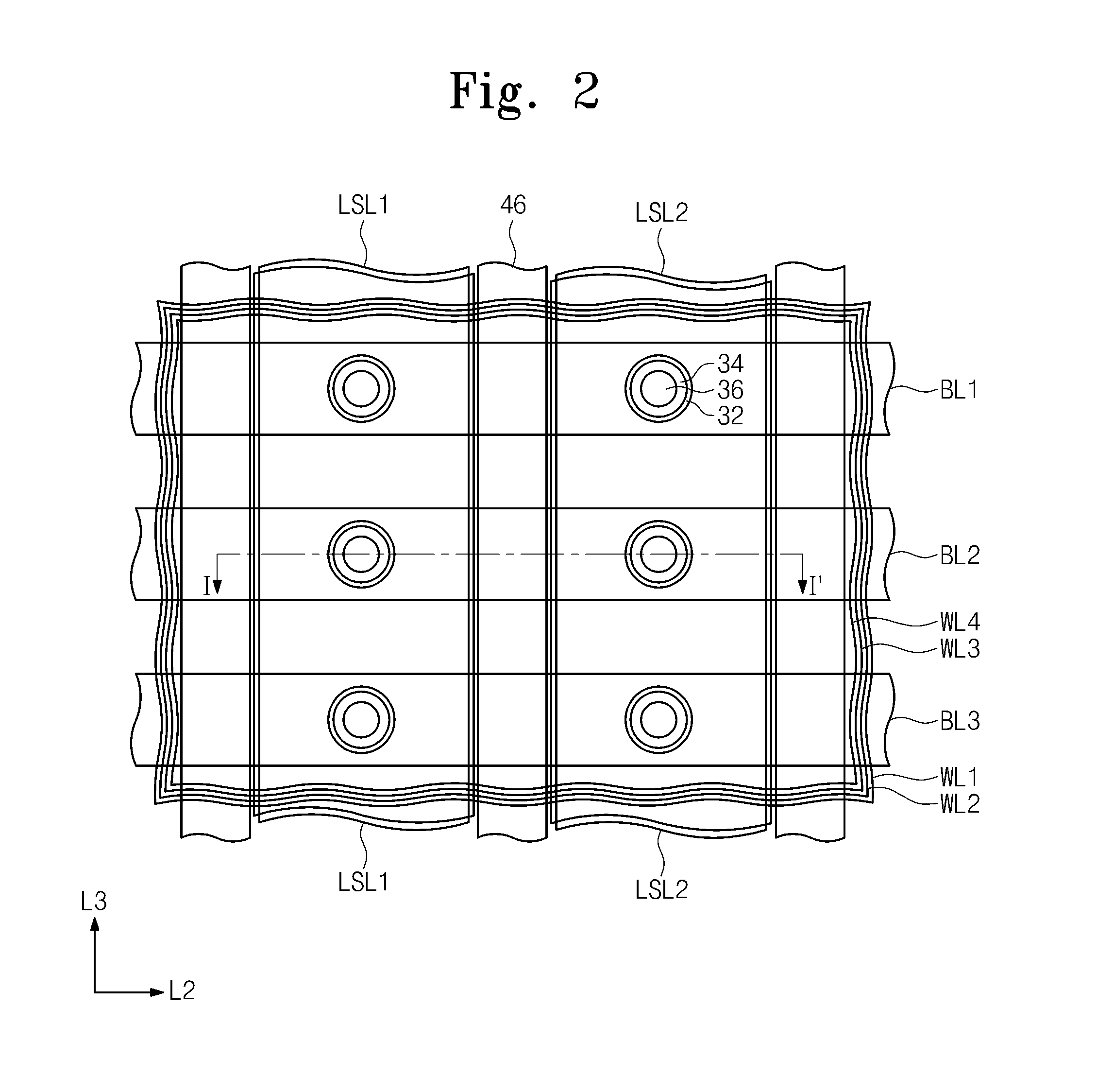
[0150]FIG. 1 is a schematic circuit diagram illustrating a resistive RAM device according to some embodiments of the present inventive concepts, and FIG. 2 is a plan view illustrating a resistive RAM device according to a first embodiment. Further, FIG. 3 is a cross-sectional view taken along a line I-I′ of FIG. 2.
[0151]Referring to FIGS. 1, 2 and 3, a resistive RAM device according to an example embodiment may include common source lines CSL, bit lines BL1, BL2 and BL3, and cell strings CSTR disposed between the common source lines CSL and the bit lines BL1, BL2 and BL3.
[0152]In some embodiments, the common source lines CSL may be disposed in or on a substrate 1. In various embodiments, the substrate 1 may comprise a semiconductor substrate or an epitaxial layer disposed on a semiconductor substrate. The common source lines CSL may comprise impurity regions disposed in the substrate 1. The common source lines CSL may have a different conductivity type from the substrate 1. In some ...
second embodiment
[0202]FIG. 16 is a cross-sectional view illustrating a resistive RAM device according to a second embodiment of the present inventive concepts.
[0203]Referring to FIG. 16, the present embodiment is different from the previous embodiment illustrated in FIG. 3 in terms of a shape of the variable resistive patterns 34. That is, the resistive RAM device according to the present embodiment may include spacer-shaped variable resistive patterns 34 covering only inner sidewalls of the active pillars 32, and not a bottom surface of the active pillars. In this manner, the resulting variable resistive patterns 34 are generally cylindrical in shape, and not cup-shaped as shown in the embodiment of FIG. 15
[0204]The resistive RAM device according to the present embodiment may be fabricated by forming the active layer 32 and the variable resistive layer 34 as illustrated in FIG. 10, by anisotropically etching the variable resistive layer 34 to form the spacer-shaped variable resistive patterns 34 a...
third embodiment
[0205]FIG. 17 is a cross-sectional view illustrating a resistive RAM device according to a third embodiment of the present inventive concepts.
[0206]Referring to FIG. 17, a resistive RAM device according to the present embodiment may include active pillars 32 and a gate insulation layer 42. Each of the active pillars 32 may include a first active layer 32a and a second active layer 32b, and the gate insulation layer 42 may include a first gate insulation layer 42a and a second gate insulation layer 42b. The first gate insulation layer 42a may cover a sidewall of the active hole 30 and may have a spacer shape. Further, the first gate insulation layer 42a may have an L-shaped cross section. The first gate insulation layer 42a may also cover sidewalls of the interlayer insulation layers 11-17 in the active hole 30. The second gate insulation layer 42b may extend in a horizontal direction to be vertically positioned between the interlayer insulation layers 11-17 and the lines LSL1-LSL2, ...
PUM
 Abstract
Description
Claims
Application Information