Bias current compensation device and method

a compensation device and bias current technology, applied in the direction of resistance/reactance/impedence, measurement devices, instruments, etc., can solve the problems of measurement errors confounding efforts to calibrate electronic components, measurement errors can include errors, etc., and achieve the effect of reducing the resistance of the variable resistan

Inactive Publication Date: 2010-06-08
MARVELL INT LTD
View PDF4 Cites 6 Cited by
  • Summary
  • Abstract
  • Description
  • Claims
  • Application Information

AI Technical Summary

Benefits of technology

[0009]The state adjuster can include a decoder that can receive a reference voltage and can generate an initial resistance of the variable resistance. The state adjuster can also include a counter that can decrease the resistance of the variable resistance from the initial resistance until the comparator determines that the sense current is substantially equal to a predetermined current. The counter can be coupled to the variable resistance and can control the variable resistance and thereby control the bias current passing through the bias-able device. The counter can decrease the resistance of the variable resistance from the initial resistance based on a clock signal. The variable resistance can include a first variable resistance, which can pass both the sense current and the first current, coupled in series to a first terminal of the bias-able device, and a second variable resistance, which can pass a residual current less than the sense current, coupled in series to a second terminal of the bias-able device.

Problems solved by technology

Because a measurement device can perturb the electronic component being measured, the measurements can include error.
Measurement errors can confound efforts to calibrate an electronic component.

Method used


Image

  • Bias current compensation device and method
  • Bias current compensation device and method
  • Bias current compensation device and method

Examples


Embodiment Construction

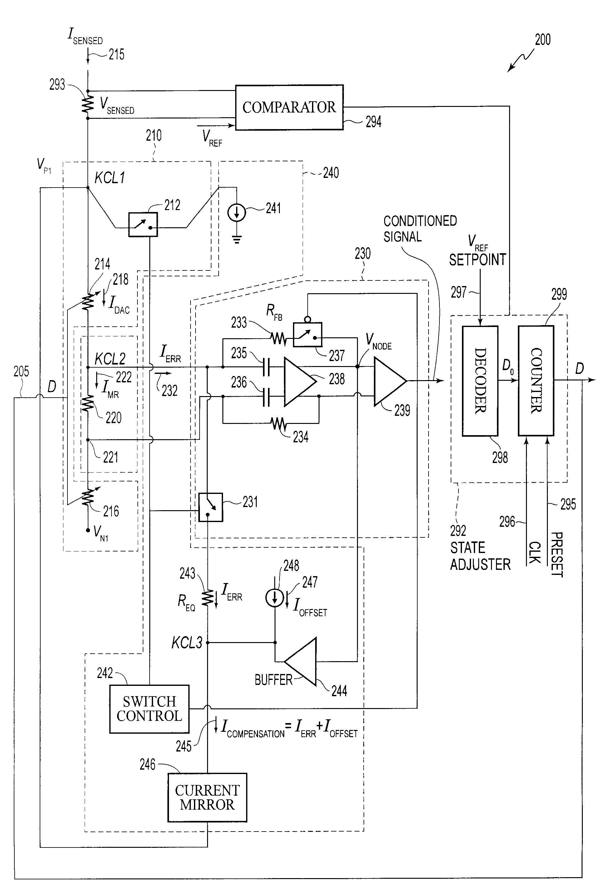
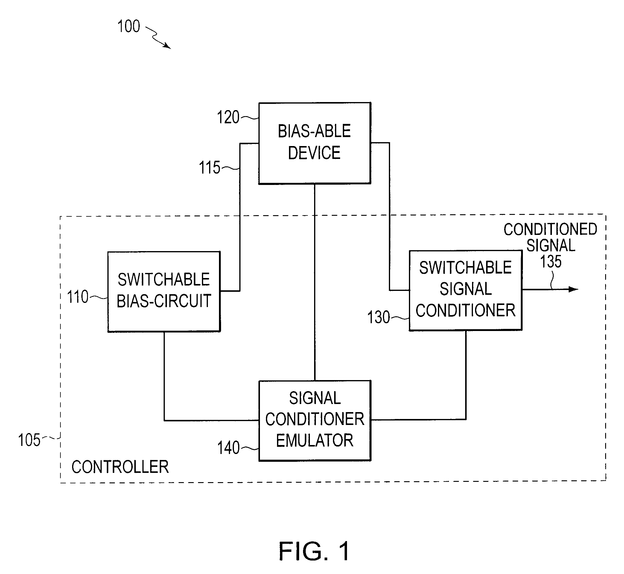
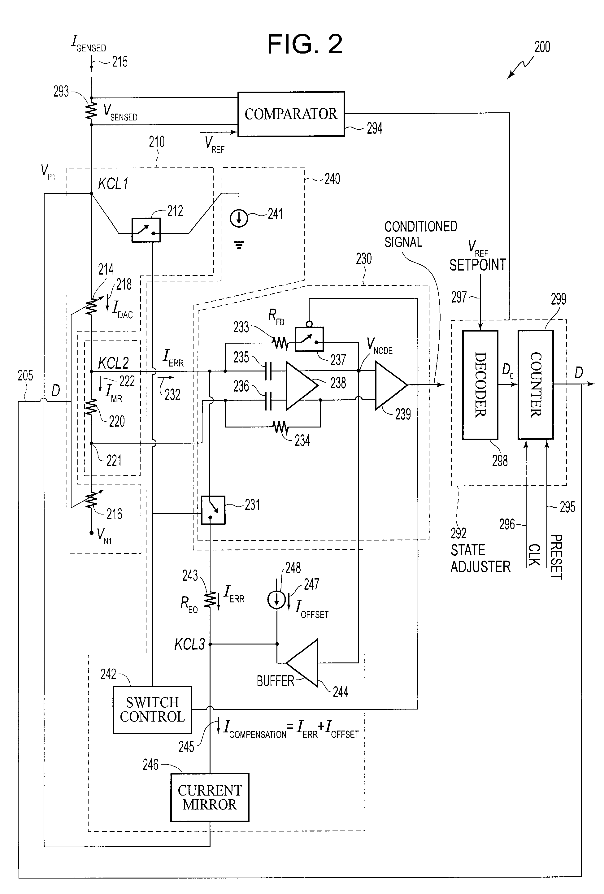
[0019]FIG. 1 shows an exemplary diagram of an input bias current compensation device and method 100 that includes a switchable bias circuit 110, a bias-able device 120, a switchable signal conditioner 130, and a signal conditioner emulator 140. Each of the elements of the input bias current compensation device and a method 100 can be coupled as shown in FIG. 1.

[0020]The switchable bias circuit 110 can accept an input from signal conditioner emulator 140 and can set a bias current to bias-able device 120 and can output a sense signal 115. In an exemplary case, the bias current can be 1 mA. The signal conditioner emulator 140 can provide a compensation current to switchable bias circuit 110.

[0021]Bias-able device 120 may be set to a bias current and can emit or receive signals. The sensitivity, efficiency, gain, signal to noise ratio, noise temperature, reliability or any parameter of bias-able device 120 can be a function of input from switchable bias circuit 110. Bias-able device 12...


PUM


Abstract

A compensation device that can include a bias-able device, a bias circuit that provides the bias-able device with a bias current, a signal conditioner selectively coupled to the bias-able device, and an emulator. The signal conditioner and emulator can divert current from the bias-able device in an operational and calibration mode, respectively. In calibration mode, the emulator generates a compensation current that is combined with a sense current so that the sense current equals the bias current.

Description

INCORPORATION BY REFERENCE[0001]This application claims the benefit of U.S. Provisional Application No. 60 / 864,041, “Way to Subtract Away the Error from Reader Amplifier When Doing MR Current Bias Calibration” filed on Nov. 2, 2006, including all cited references which are hereby incorporated herein by reference in their entirety.CROSS-REFERENCE TO RELATED APPLICATIONS[0002]Cross-reference is made to the following co-pending and commonly assigned U.S. patent application: 11 / 931,422, “Bias Setting Device”. The entire disclosure of the above-identified co-pending Application is hereby incorporated herein by reference in its entirety.BACKGROUND[0003]Electronic components are often operated or tested at a given condition despite intrinsic component variability. Also, the variability itself may be of interest, such as when one measures a component property like resistance or capacitance. Because a measurement device can perturb the electronic component being measured, the measurements ca...

Claims


Application Information

Patent Timeline
Patent Type & Authority Patents(United States)
IPC IPC(8): G05F1/10
CPCG01R27/14G01R35/005
Inventor LI, KAN
Owner MARVELL INT LTD
Why Eureka
Try Eureka