LED package with multiple element light source and encapsulant having planar surfaces

Active Publication Date: 2013-12-12
CREELED INC
View PDF13 Cites 89 Cited by
  • Summary
  • Abstract
  • Description
  • Claims
  • Application Information

AI Technical Summary

Benefits of technology

[0012]The present invention is generally directed to LED packages that are compact and efficiently emit light, and can comprise encapsulants with planar surfaces that refract and/or reflect light within the package encapsulant. The packages can also comprise a submount with a plurality of LEDs and a blanket conversion material layer on one or more of the LEDs. The blanket conversion material may also cover at least part of the submount. The encapsulant can be on the submount, over the LEDs, and over at least part of the bl

Problems solved by technology

However, such lamps are highly inefficient light sources, with as much as 95% of the input energy lost, primarily in the form of heat or infrared energy.
One common alternative to incandescent lamps, so-called compact fluorescent lamps (CFLs), are more effective at converting electricity into light but require the use of toxic materials which, along with its various compounds, can cause both chronic and acute poisoning and can lead to environmental pollution.
While the reflective cup 13 may direct light

Method used


Image

  • LED package with multiple element light source and encapsulant having planar surfaces
  • LED package with multiple element light source and encapsulant having planar surfaces
  • LED package with multiple element light source and encapsulant having planar surfaces

Examples


Embodiment Construction

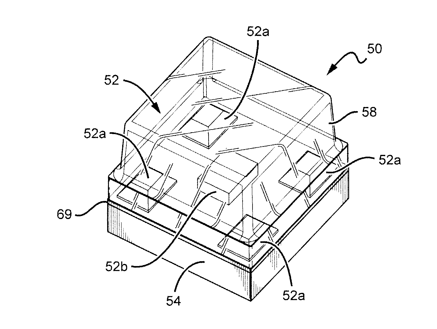
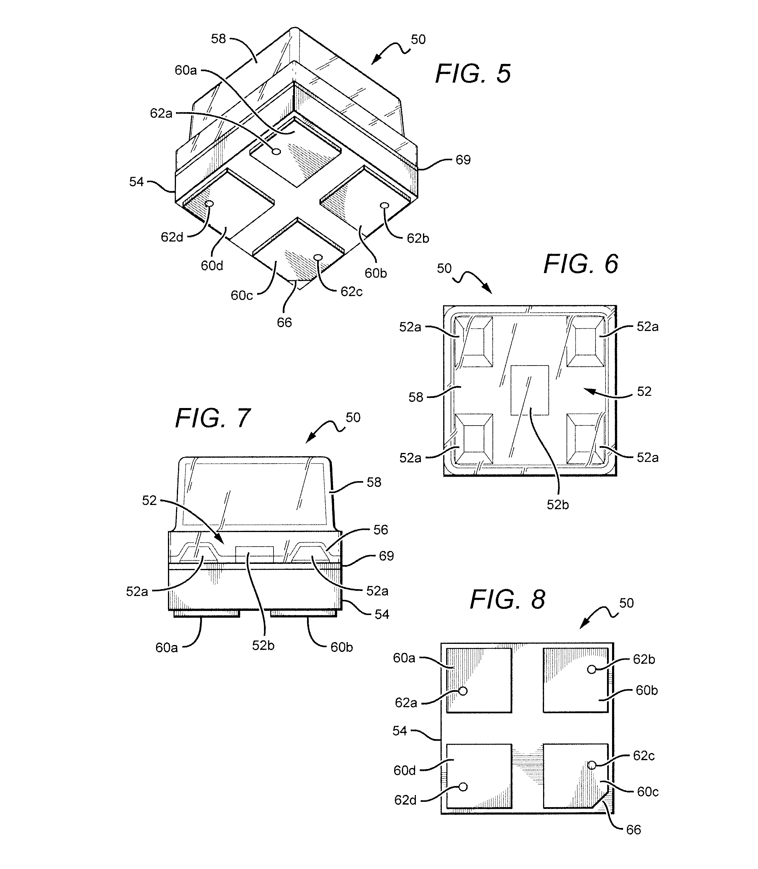
[0059]The present invention is directed to different embodiments of LED package structures having a light source that comprises a plurality of LED chips. The LED packages can be arranged in different ways and are relatively small, while at the same time are efficient, reliable and cost effective. Some embodiments according to the present invention, can emit with same or similar efficiency to a similar LED packages with hemispheric encapsulants, but can be smaller and less expensive to manufacture.

[0060]The packages according to the present invention can provide these improvements by having conversion material and encapsulants that are arranged and shaped to capitalize on the total internal reflection (TIR) of light within the package. That is, the encapsulant can be shaped such that light incident on the package encapsulant at angles greater than the critical angle for TIR can be reflected back towards a conversion material within the package such that the light is converted or “rec...


PUM


Abstract

LED packages are disclosed that are compact and efficiently emit light, and can comprise encapsulants with planar surfaces that refract and/or reflect light within the package encapsulant. The packages can comprise a submount with a plurality of LEDs, which emit different colors of light, and a blanket conversion material layer on the LEDs and the submount. The encapsulant can be on the submount, over the LEDs, and light reflected within the encapsulant will reach the conversion material to be absorbed and emitted omnidirectionally. Reflected light can now escape the encapsulant, allowing for efficient emission and a broader emission profile, when compared to conventional packages with hemispheric encapsulants or lenses. The LED package can have a higher chip area to LED package area ratio. By using an encapsulant with planar surfaces, the LED package provides unique dimensional relationships between the features and LED package ratios, enabling more flexibility with different applications.

Description

[0001]This application claims the benefit of U.S. Provisional Patent Application Ser. No. 61 / 658,271, filed on Jun. 11, 2012, U.S. Provisional Patent Application Ser. No. 61 / 660,231, filed on Jun. 15, 2012, and U.S. Provisional Patent Application Ser. No. 61 / 696,205, filed on Sep. 2, 2012.BACKGROUND OF THE INVENTION[0002]1. Field of the Invention[0003]This invention pertains to solid state light emitters and in particular to light emitting diode (LED) packages with multiple LEDs, with the packages capable of producing high efficiency light emission with a wider emission pattern from a device with smaller footprint.[0004]2. Description of the Related Art[0005]Incandescent or filament-based lamps or bulbs are commonly used as light sources for both residential and commercial facilities. However, such lamps are highly inefficient light sources, with as much as 95% of the input energy lost, primarily in the form of heat or infrared energy. One common alternative to incandescent lamps, s...

Claims


Application Information

Patent Timeline
IPC IPC(8): H01L33/50H01L33/54
CPCH01L33/502H01L33/54H01L33/505H01L2224/73265H01L2224/48091H01L2224/48247H01L2924/00014H01L2924/181F21V9/00H01L2924/00012H01L2924/0002H01L33/504H01L33/60H01L2924/00
Inventor LOWES, THEODORETARSA, ERIC J.HEIKMAN, STENKELLER, BERNDREIHERZER, JESSEBENJAMIN, HORMOZ
Owner CREELED INC
Why Eureka
Try Eureka