

Method of manufacturing nitride semiconductor template
- Summary
- Abstract
- Description
- Claims
- Application Information
AI Technical Summary
Benefits of technology
Problems solved by technology
Method used
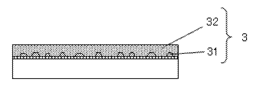
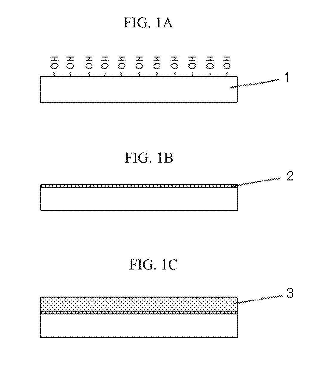
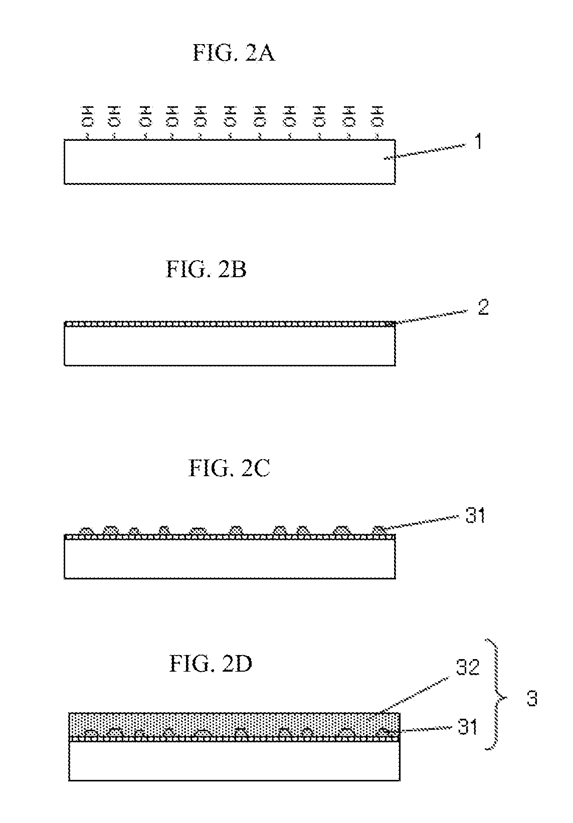
Image

Examples
example 1
Contacting
[0041]The reactor under a normal pressure was filled with nitrogen gas whose water vapor concentration was 5 μmol / L. As the base substrate, a sapphire substrate whose diameter was about 7.6 cm (3 inches) was placed on a tray in the reactor with its C-plane facing up, and brought into contact with water vapor in the reactor for 10 minutes. During the step of contacting, the inside of the reactor was maintained at a normal temperature.
Thermally Cleaning
[0042]After the step of contacting, the atmosphere inside the reactor was replaced by nitrogen. After the replacement, the reactor was adjusted so that the temperature of the tray became 1200° C. After the adjustment, hydrogen gas and nitrogen gas were continuously supplied to the reactor for 30 minutes at the flow rate of 0.31 mol / min (7 slm) and 0.13 mol / min (3 slm), respectively. Thus, the sapphire substrate was thermally cleaned.
Nitiriding
[0043]After the step of thermally cleaning, the pressure in the reactor was reduced, ...
example 2
[0047]A nitride semiconductor template was obtained in the same manner as in Example 1 except that nitrogen gas whose water vapor concentration was 10 μmol / L was used in the step of contacting.
PUM
 Abstract
Description
Claims
Application Information