Ultraviolet light emitting device

Active Publication Date: 2016-10-13
PANASONIC INTELLECTUAL PROPERTY MANAGEMENT CO LTD
View PDF0 Cites 3 Cited by
  • Summary
  • Abstract
  • Description
  • Claims
  • Application Information

AI Technical Summary

Benefits of technology

[0117]The characteristics and advantages of the ultraviolet light emitting device 1 according to the present embodiment will be described below.
[0118]In an ultraviolet light emitting device that includes a dielectric layer formed of low-melting-point glass, it is difficult to efficiently emit deep ultraviolet light generated by the light-emitting layer from opposite sides of the ultraviolet light emitting device. This is because the dielectric layer absorbs most of the deep ultraviolet light and thereby reduces the amount of deep ultraviolet light emitted from the side on which the dielectric layer is located.
[0119]In order to solve the problem, the ultraviolet light emitting device 1 according to the present embodiment includes the first substrate 10, the electrodes 20 located directly or indirectly on the main surface of the first substrate 10, the dielectric layer 30 that is located in the first regions 92 directly or indirectly on the main surface of the first substrate 10 in such a manner as to cover the electrodes 20 and is not located in the second regions 93 directly or indirectly on the main surface of the first substrate 10 different from the first regions 92, the first regions 92 including a region in which the electrodes 20 are located, the second substrate 11 facing the main surface of the first substrate 10, and the light-emitting layer 40 that is located in the second regions 93 and emits ultraviolet light. The first substrate 10 and the second substrate 11 are composed mainly of a material that is transparent to ultraviolet light. The discharge space 12 between the first substrate 10 and the se

Problems solved by technology

For lithography, which requires wide and uniform intensity ligh

Method used


Image

  • Ultraviolet light emitting device
  • Ultraviolet light emitting device
  • Ultraviolet light emitting device

Examples


embodiments

1. Structure

1-1. Outline

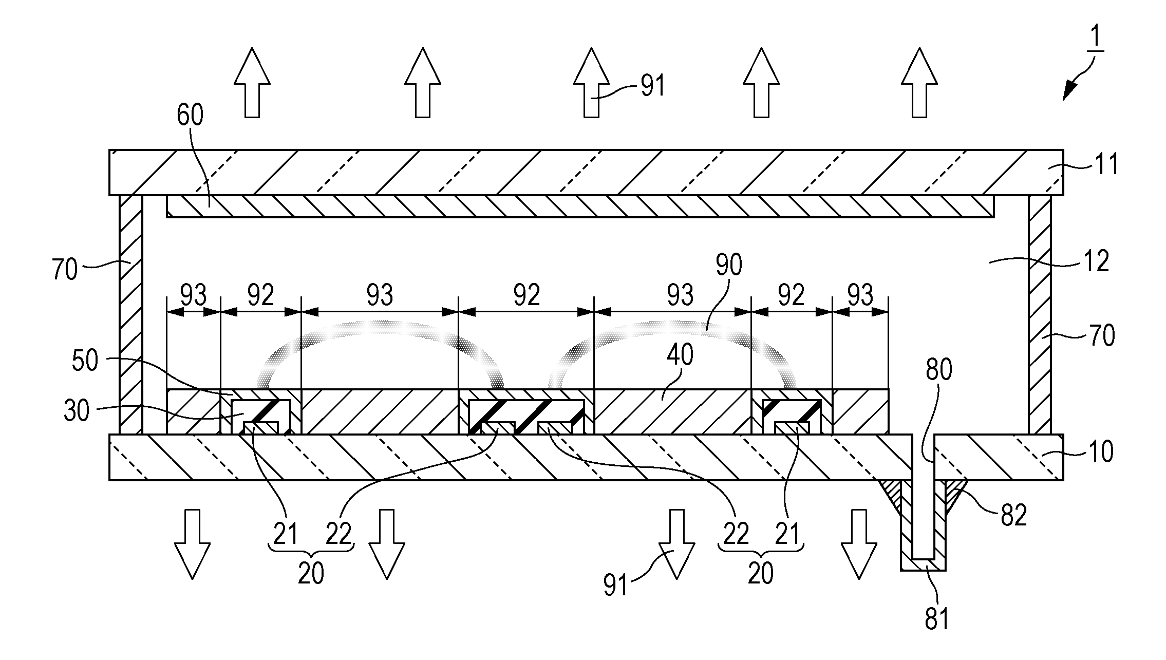
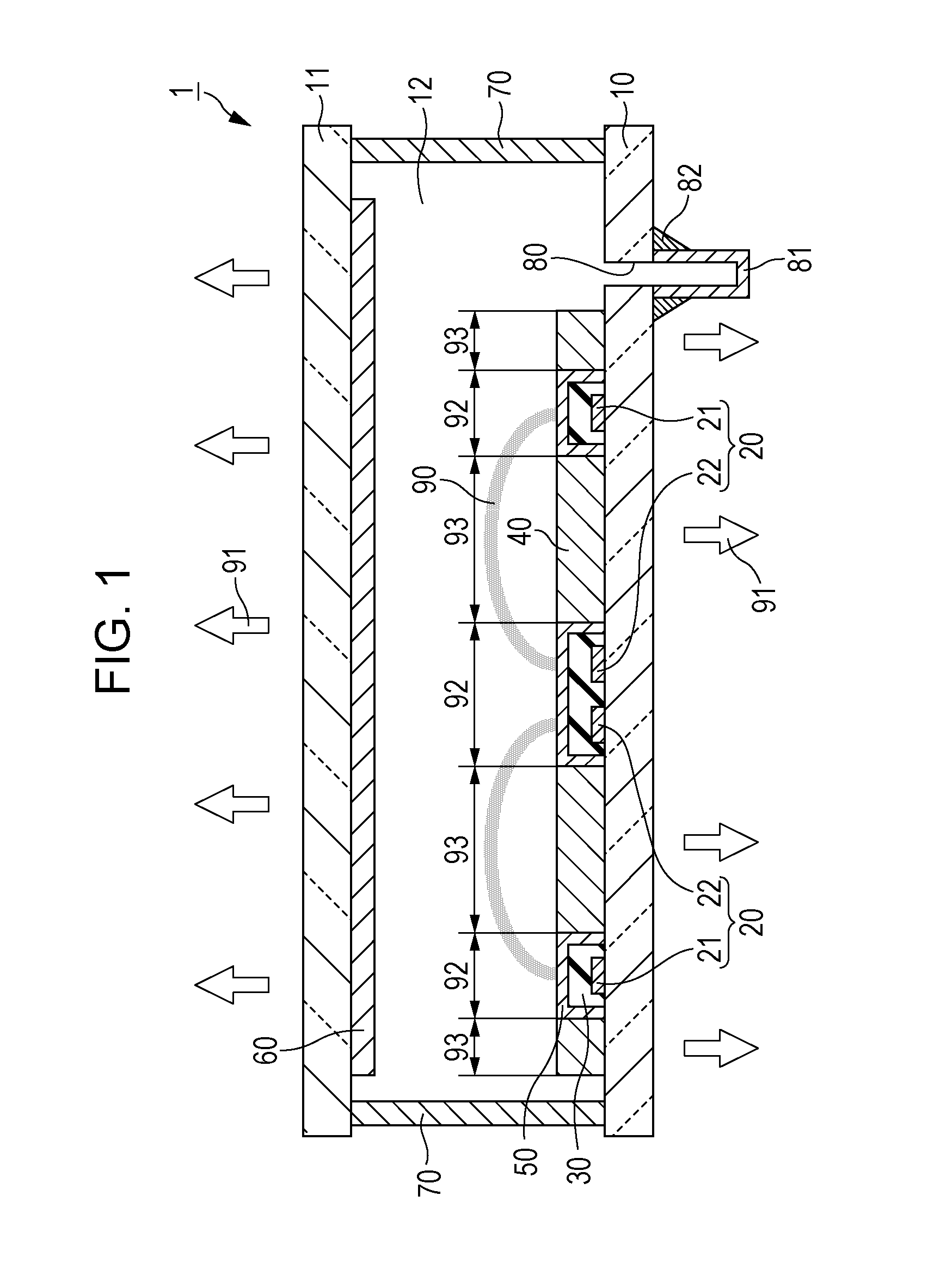
[0046]An ultraviolet light emitting device according to one embodiment of the present disclosure will be described below with reference to FIG. 1. FIG. 1 is a schematic cross-sectional view of an ultraviolet light emitting device 1 according to the present embodiment.

[0047]In the ultraviolet light emitting device 1, a phosphor is used in combination with barrier discharge. As illustrated in FIG. 1, the ultraviolet light emitting device 1 includes a first substrate 10, a second substrate 11, electrodes 20, a dielectric layer 30, a light-emitting layer 40, a protective layer 50, a light-emitting layer 60, a sealing member 70, and a tip tube 81.

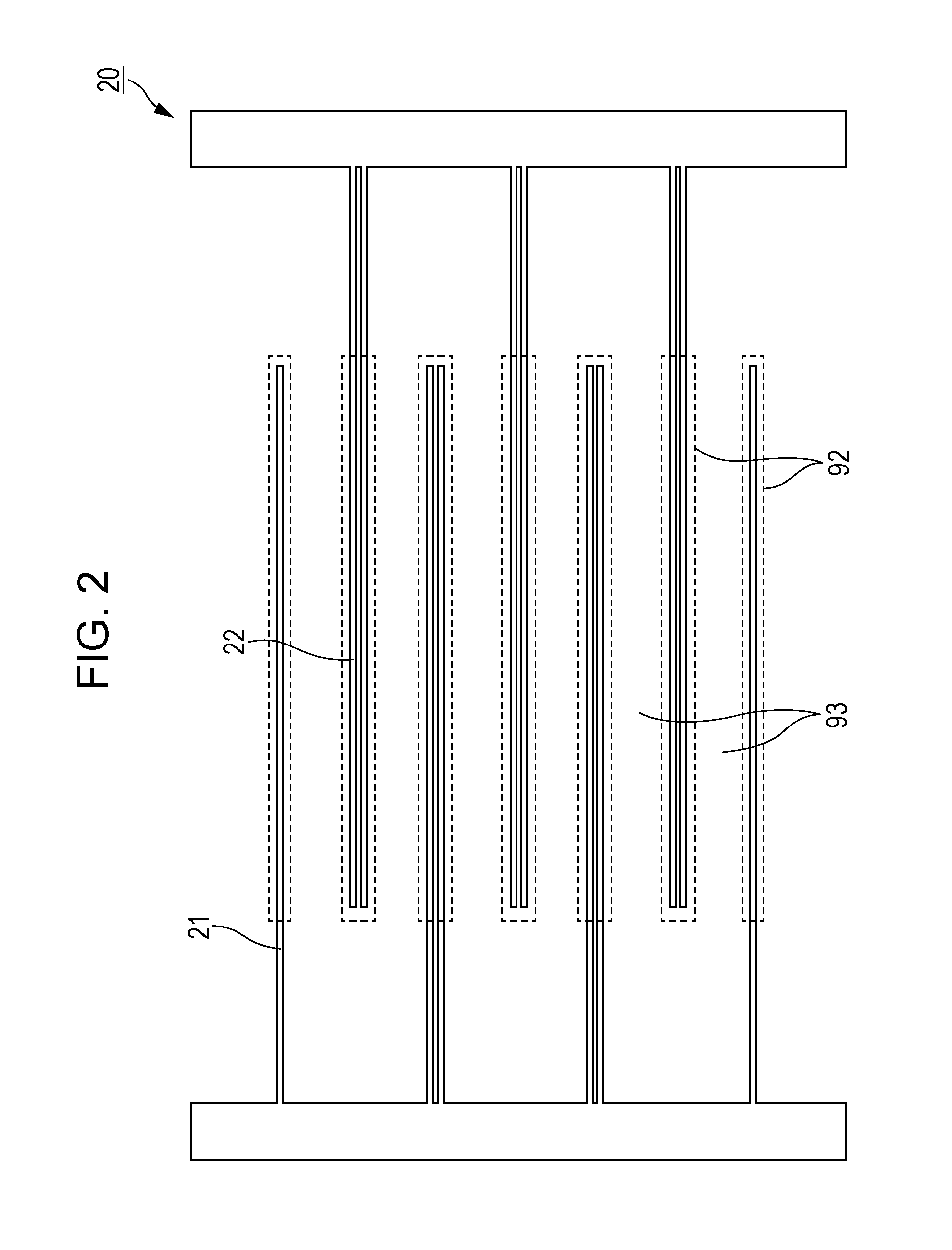
[0048]In the ultraviolet light emitting device 1, the first substrate 10 and the second substrate 11 are joined together with the sealing member 70, thus forming a discharge space 12. The electrodes 20 to which a voltage is applied to cause electrical discharge 90 are located on the first substrate 10 and are covered with...


PUM


Abstract

An ultraviolet light emitting device includes: a first substrate; a second substrate; a gas in a space between the first substrate and the second substrate; electrodes directly or indirectly on a first main surface of the first substrate; a dielectric layer that is located in a first region directly or indirectly on the first main surface of the first substrate and covers the electrodes, the dielectric layer being not located in a second region directly or indirectly on the first main surface of the first substrate, the second region being different from the first region, the first region including regions in which the electrodes are located; and a light-emitting layer that is located in the second region and/or located directly or indirectly on at least one of second and third main surfaces of the second substrate and emits the ultraviolet light in the gas due to electrical discharge between the electrodes.

Description

BACKGROUND[0001]1. Technical Field[0002]The present disclosure relates to an ultraviolet light emitting device.[0003]2. Description of the Related Art[0004]Deep ultraviolet light having a wavelength of approximately 200 to 350 nm is utilized in various fields of sterilization, water purification, lithography, and illumination. Hitherto, mercury lamps have been widely used as deep ultraviolet light sources. Mercury lamps utilize a mercury glow discharge. From the perspective of the reduction of load on the environment, however, regulations for environmentally hazardous substances, such as mercury, are being tightened up, as in WEEE & RoHS directives in Europe. Thus, there is a demand for alternative light sources to mercury lamps. Mercury lamps are point emission sources. For lithography, which requires wide and uniform intensity light, therefore, mercury lamps require complex light source design.[0005]An example of deep ultraviolet light sources free of mercury may be a deep ultravi...

Claims


Application Information

Patent Timeline
IPC IPC(8): H01J61/44H01J65/00H01J61/16
CPCH01J61/44H01J65/00H01J61/16H01J61/302H01J61/305
Inventor ZUKAWA, TAKEHIROSASAKI, YOSHIKINAGAO, NOBUAKI
Owner PANASONIC INTELLECTUAL PROPERTY MANAGEMENT CO LTD
Why Eureka
Try Eureka