Detector and inspecting apparatus

Active Publication Date: 2009-09-10
EBARA CORP
View PDF7 Cites 36 Cited by
  • Summary
  • Abstract
  • Description
  • Claims
  • Application Information

AI Technical Summary

Benefits of technology

[0032]In the inspecting apparatus according to the present invention, a beam irradiated to a sample may be an electron beam or light such as UV light, DUV light, laser light or the like, or a combination of an electron beam and light. Any of reflected electrons, secondary electrons, back scattered electrons, and Auger electrons may be used for the electron beams to capture a required image. When using light such as UV light, DUV light, laser light or the like, an image is detected by optical electrons. It is also possible to detect defects on the surface of a sample using scattered light which occurs when such light is irradiated to the surface of the sample. A quartz fiver or a hollow fiber can be used to efficiently introduce light such as UV light, DUV light, laser light or the like onto the surface of the sample.
[0033]When a combination of an electron beam and light is used for irradiating the surface of a sample therewith, it is poss

Problems solved by technology

Specifically, when the incident conditions are adjusted using the TDI sensor, a low scaling factor of image in the adjustments of the incident condition causes secondary electrons from a sample to impinge and not impinge on some regions of a MCP (micro-channel plate), which receives secondary electrons from a sample, resulting in local damages to the MCP.
However, a problem arises in deterioration of MTF due to the feed throu

Method used


Image

  • Detector and inspecting apparatus
  • Detector and inspecting apparatus
  • Detector and inspecting apparatus

Examples


Example

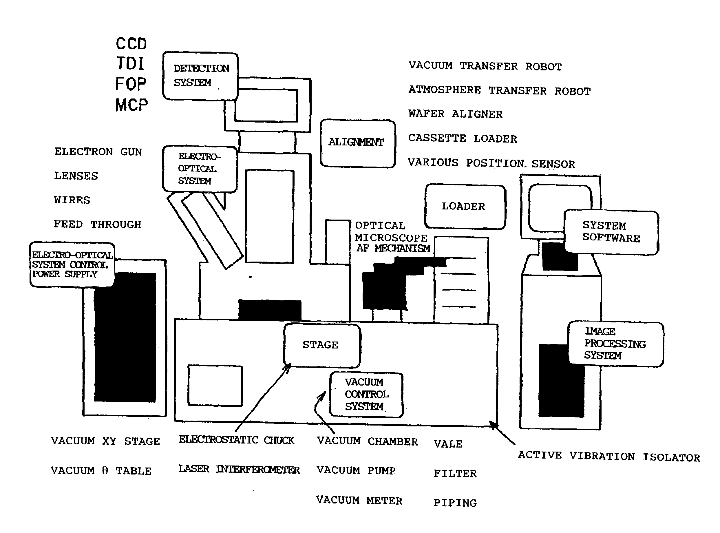
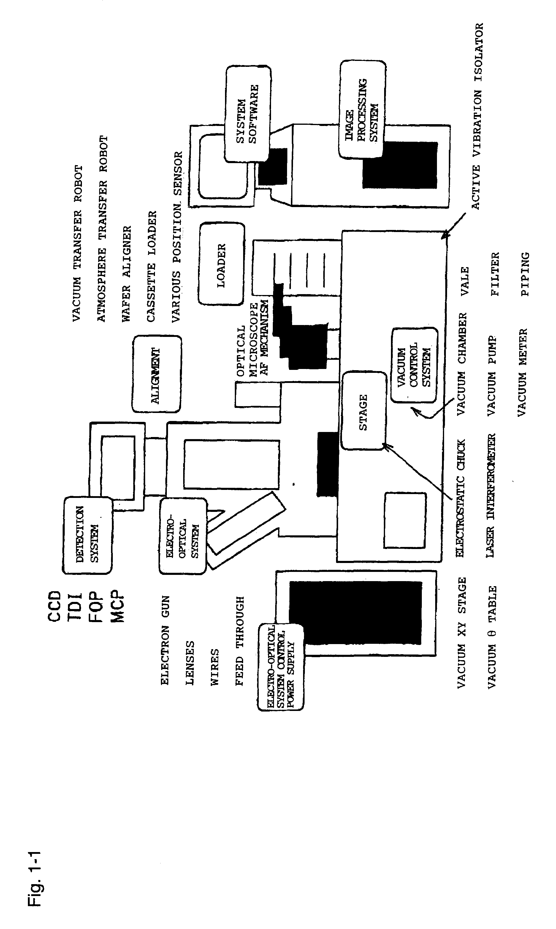
[0149]FIG. 3 is a diagram schematically showing a first embodiment of the inspecting apparatus according to the present invention, which comprises a detector having an electron sensor and a detector having an optical sensor both contained in a single chamber. In FIG. 3, a CCD detector 11 and a TDI detector 12 are disposed within a vacuum chamber MC such that an EB-CCD (electron bombardment charge coupled device) sensor 13 of the CCD detector 11 is positioned closer to a sample. In FIG. 3, the CCD detector 11 and TDI detector 12 have their electron incident plane perpendicular to the drawing. The EB-CCD sensor 13 is supported such that it can be translated in the left-to-right direction in the figure by a moving mechanism M disposed outside of the vacuum chamber MC. In this way, the EB-CCD sensor 13 can be selectively moved to a position at which it receives an electron beam e, and to a position at which it directly applies the electron beam e into the TDI detector 12, thus making it...

Example

[0155]FIG. 4 is a diagram schematically showing a second embodiment of an inspecting apparatus according to the present invention. The moving mechanism M shown in FIG. 3 can simply translate in one axial direction (for example, in the X-direction). Instead, in the second embodiment shown in FIG. 4, the moving mechanism M is configured to be movable in three axial directions (X-, Y-, and Z-directions), to finely adjust the center of the EB-CCD sensor 13 with respect to the center of the optical axis of the electro-optical system. In this regard, an electron deflection mechanism may be provided in front of the EB-sensor 13 (closer to a sample) to adjust the position of the electron beam in order to adjust the optical axis of the electro-optical system.

Example

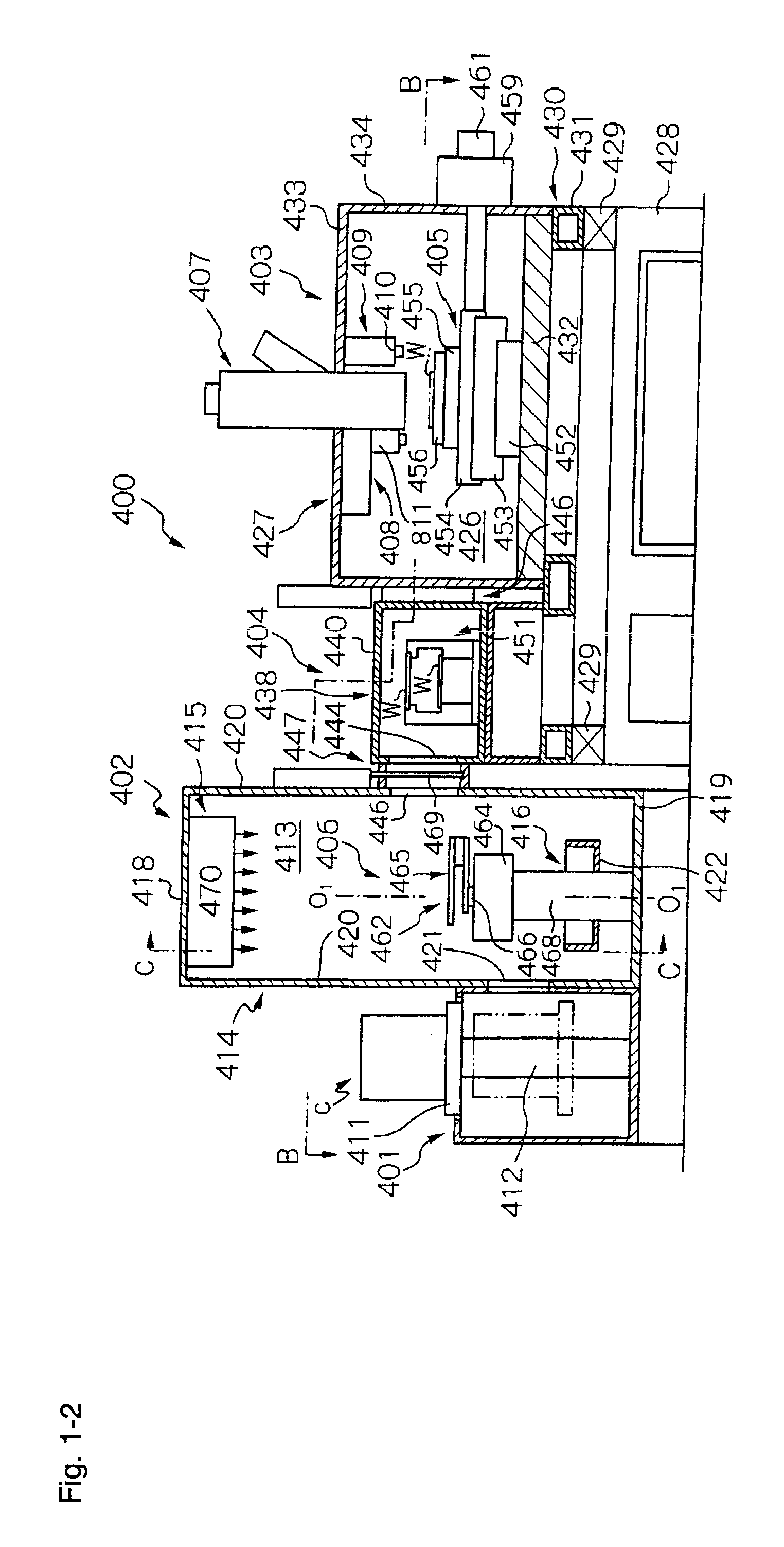
[0156]FIGS. 5(A)-5(C) schematically shown a third embodiment of an inspecting apparatus according to the present invention, where (A) is a view taken from the front, and (B) and (C) are views taken from one side. As shown, the moving mechanism M in this embodiment utilizes rotational movements rather than movements in one axial or three axial directions. It should be noted that the TDI detector 12 does not comprise the MCP because the electron amplification is not needed in this embodiment.

[0157]In FIG. 5(A), one end of a rotary shaft 21 is coupled to one end of a flat EB-CCD sensor 13 which contains required circuits, substrates and the like, while the other end of the rotary shaft 21 is coupled to the moving mechanism M. FIGS. 5(B) and 5(C) are views of the configuration shown in FIG. 5(A), taken from the side closer to the moving mechanism M. When the CCD detector 11 is used, the EB-CCD sensor 13 is moved such that the sensor plane thereof is perpendicular to the electron beam e,...


PUM


Abstract

An inspecting apparatus for reducing a time loss associated with a work for changing a detector is characterized by comprising a plurality of detectors 11, 12 for receiving an electron beam emitted from a sample W to capture image data representative of the sample W, and a switching mechanism M for causing the electron beam to be incident on one of the plurality of detectors 11, 12, where the plurality of detectors 11, 12 are disposed in the same chamber MC. The plurality of detectors 11, 12 can be an arbitrary combination of a detector comprising an electron sensor for converting an electron beam into an electric signal with a detector comprising an optical sensor for converting an electron beam into light and converting the light into an electric signal. The switching mechanism M may be a mechanical moving mechanism or an electron beam deflector.

Description

TECHNICAL FIELD[0001]The present invention relates a detector for capturing electron beams or optical signals. More particularly, the present invention relates to an inspecting apparatus which has two or more detectors disposed within a single barrel, one of which is selected in accordance with the amount of electronic or optical signals or an S / N ratio, thereby allowing for detection and measurement of images on the surface of a sample.[0002]With the use of this inspecting apparatus, a sample can be efficiently inspected for evaluating the structure on the surface thereof, observing the surface in enlarged view, evaluating the material thereof, inspecting an electrically conductive state thereof, and the like. Accordingly, the present invention relates to a method of accurately and reliably inspecting highly dense patterns having a minimum line width of 0.15 μm or less for defects at a high throughput, and a device manufacturing method which involves inspecting patterns halfway in ...

Claims


Application Information

Patent Timeline
IPC IPC(8): G01N23/00G01N23/225G01N21/00
CPCH01J37/244H01J37/28H01J37/261H01J2237/2446H01J2237/2441G01R31/302H01J37/29H01L22/00
Inventor HATAKEYAMA, MASAHIROYOSHIKAWA, SHOJISUEMATSU, KENICHIKARIMATA, TSUTOMUNOJI, NOBUHARU
Owner EBARA CORP
Why Eureka
Try Eureka