Edge Protection of Bonded Wafers During Wafer Thinning

a technology of thinning process and edge protection, which is applied in the direction of semiconductor devices, semiconductor/solid-state device details, electrical apparatus, etc., can solve the problems of thinning process and thinning process, and can be very risky, and achieve the effect of preventing the thinning process from affecting the surface of the carrier wafer and the dielectric film

Inactive Publication Date: 2013-12-12
GLOBALFOUNDRIES US INC
View PDF10 Cites 33 Cited by
  • Summary
  • Abstract
  • Description
  • Claims
  • Application Information

AI Technical Summary

Benefits of technology

[0003]The various advantages and purposes of the exemplary embodiments as described above and hereafter are achieved by providing, according to a first aspect of the exemplary embodiments, a method of edge protecting bonded semiconductor wafers comprising: providing a second semiconductor wafer having a first surface and a second surface opposite to the first surface; attaching the first surface of the first semiconductor wafer to a first semiconductor wafer by using a bonding layer/interface; thinning the second semiconductor wafer from the second surface to a first predetermined dimension; forming a first protective layer to entirely cover the second semiconductor wafer and at least a portion of an edge of the first semiconductor wafer; thinning the second semiconductor wafer from the second surface to a second predetermined dimension while maintaining the first protective layer on an edge of the second semiconductor wafer and the edge of the first semiconductor wafer; providing a third semiconductor wafer having a first surface and a second surface opposite to the first surface; attaching the first surface of the third semiconductor wafer to the second surface of the second semiconductor wafer by using a bonding layer/interface, the third semiconductor wafer, second semiconductor wafer and first semiconductor wafer forming a semiconductor wafer stack; thinning the third semiconductor wafer from the second surface to a third predetermined dimension; forming a second protective layer to entirely cover the third semiconductor wafer and the first protective layer; thinning the third semiconductor wafer to a fourth predetermined dimension while maintaining the second protective layer on an edge of the third semiconductor wafer and on the first protective layer; and dicing the semiconductor wafer stack with the maintained second protective layer and first protective layer into a plurality of three dimensional chip stacks.
[0004]According to a second aspect of the exemplary embodiments, there is provided a method o

Problems solved by technology

However, grinding mechanically the top wafer to a very small thickness can be very risky and can yield to several process yield issues, such as chipping or cracking, and

Method used


Image

  • Edge Protection of Bonded Wafers During Wafer Thinning
  • Edge Protection of Bonded Wafers During Wafer Thinning
  • Edge Protection of Bonded Wafers During Wafer Thinning

Examples


Embodiment Construction

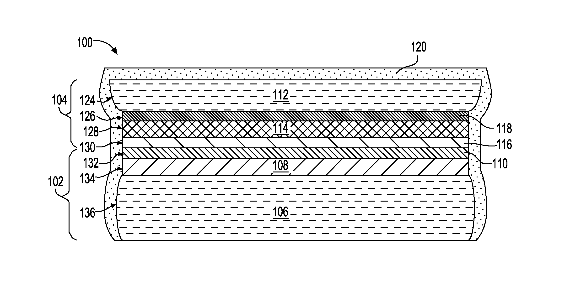
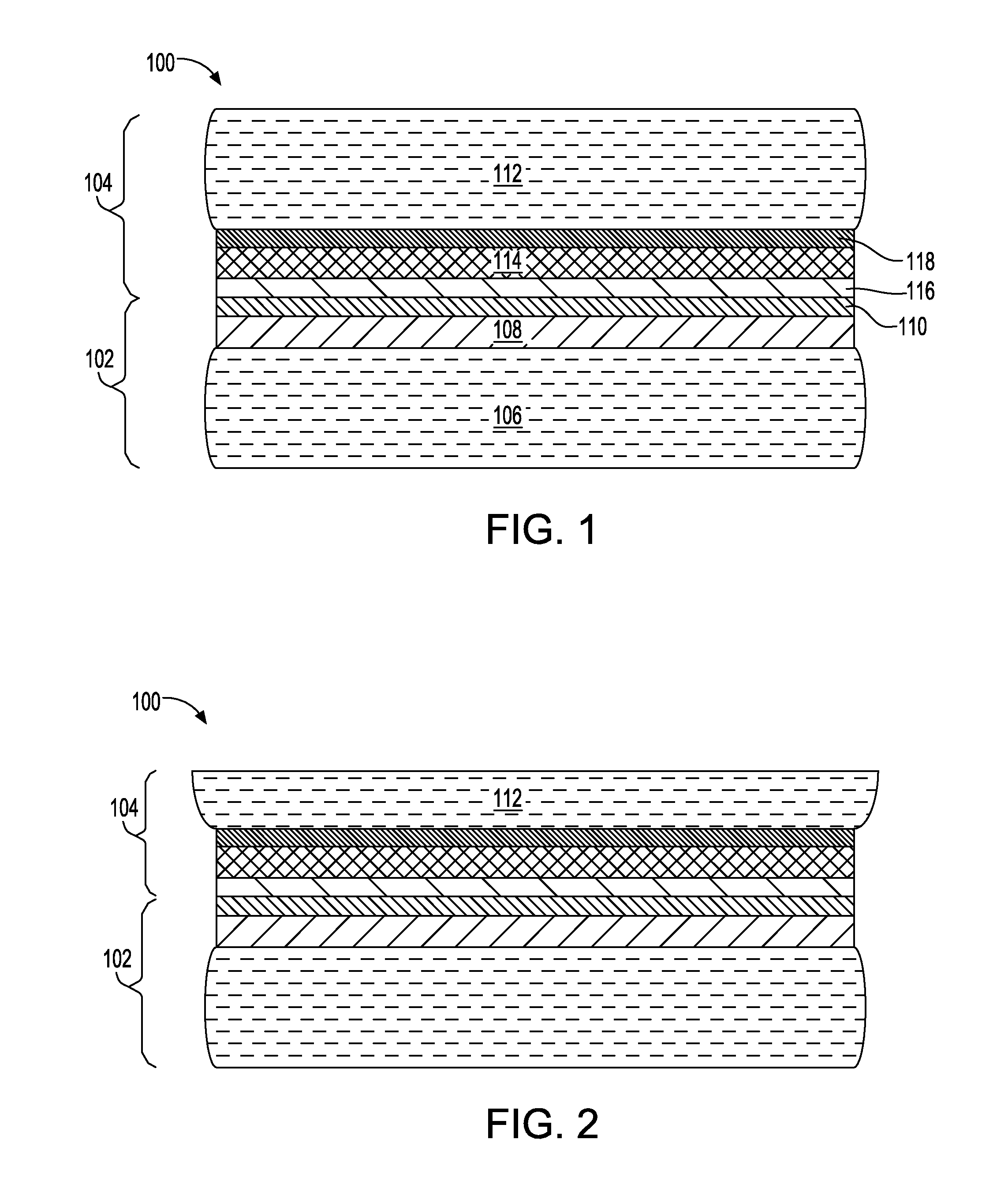
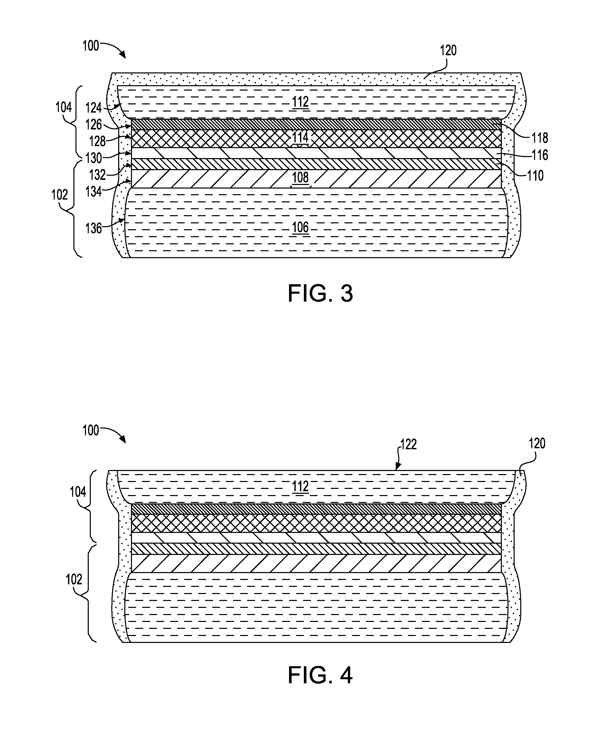
[0040]The present inventors propose to protect the edges of bonded semiconductor wafers during wafer thinning processing and subsequent processing operations until the time the semiconductor wafers are diced to form 3D semiconductor chips.

[0041]A first exemplary embodiment is illustrated in FIGS. 1 to 13.

[0042]Referring to the Figures in more detail, and particularly referring to FIG. 1, there are shown bonded semiconductor wafers 100 which may include a first semiconductor wafer 102 bonded to a second semiconductor wafer 104. The first semiconductor wafer 102 may also be referred to as a bottom wafer. First semiconductor wafer 102 includes a bulk silicon substrate 106, a device layer 108 and a bonding layer / interface 110. The device layer 108 may actually comprise several sublayers in which semiconductor devices and interconnect wiring may be formed.

[0043]Second semiconductor wafer 104 may also include a bulk silicon substrate 112, a device layer 114 and a bonding layer / interface 1...


PUM


Abstract

A method of edge protecting bonded semiconductor wafers. A second semiconductor wafer and a first semiconductor wafer are attached by a bonding layer/interface and the second semiconductor wafer undergoes a thinning process. As a part of the thinning process, a first protective layer is applied to the edges of the second and first semiconductor wafers. A third semiconductor wafer is attached to the second semiconductor wafer by a bonding layer/interface and the third semiconductor wafer undergoes a thinning process. As a part of the thinning process, a second protective layer is applied to the edges of the third semiconductor wafer and over the first protective layer. The first, second and third semiconductor wafers form a wafer stack. The wafer stack is diced into a plurality of 3D chips while maintaining the first and second protective layers.

Description

BACKGROUND[0001]The present invention relates to protecting the edge of bonded semiconductor wafers and, more particularly, relates to protecting the edge of a stack of bonded semiconductor wafers during wafer thinning.[0002]In one possible scheme for wafer-scale bonding three-dimension (3D) integration, the top wafer may be bonded face down to the bottom wafer. In general, wafer-scale bonding may be face-to-face bonding or face-to-back bonding. Subsequently, the top wafer is ground and polished from the back in order to leave a relatively thin portion of the top wafer, so that the through-silicon via definition that will facilitate electrical connection is possible. However, grinding mechanically the top wafer to a very small thickness can be very risky and can yield to several process yield issues, such as chipping or cracking, and uniformity issues regarding the remaining wafer thickness. In one possible approach to circumvent this issue, the final wafer thinning step can be done...

Claims


Application Information

Patent Timeline
IPC IPC(8): H01L23/58H01L21/30
CPCH01L23/562H01L25/0657H01L25/50H01L27/0688H01L2924/0002H01L2924/00
Inventor LA TULIPE, JR., DOUGLAS C.SKORDAS, SPYRIDONVO, TUAN A.WINSTEL, KEVIN R.
Owner GLOBALFOUNDRIES US INC
Why Eureka
Try Eureka