Light-emitting device having patterned substrate and method of manufacturing thereof

a technology of light-emitting devices and substrates, which is applied in the direction of semiconductor devices, basic electric elements, electrical devices, etc., can solve the problems of poor light extraction efficiency and heat dissipation efficiency, adversely affecting epitaxial quality, and difficulty in subsequently epitaxial growth, so as to achieve the effect of improving light extraction efficiency and improving the quality of the epitaxy layer

Active Publication Date: 2014-01-16
EPISTAR CORP
View PDF4 Cites 7 Cited by
  • Summary
  • Abstract
  • Description
  • Claims
  • Application Information

AI Technical Summary

Benefits of technology

[0007]One aspect of the disclosure proposes a light-emitting device having a patterned substrate. The patterned substrate benefits both quality of epitaxy layer and light extraction efficiency.

Problems solved by technology

It causes both the poor light extraction efficiency and the heat dissipation.
Nevertheless, the pattern on the substrate is usually formed deeper in order to compensate the light loss due to the internal total reflection effect, but the high aspect ratio of the deeper pattern on the substrate causes difficulty for subsequently epitaxial growth and adversely affects the epitaxial quality.
By this method, it is hard to control the pattern dimension such as the depth or the width.
Moreover, the epitaxy quality is poor for an epitaxial layer grown on the randomly rough surface.

Method used


Image

  • Light-emitting device having patterned substrate and method of manufacturing thereof
  • Light-emitting device having patterned substrate and method of manufacturing thereof
  • Light-emitting device having patterned substrate and method of manufacturing thereof

Examples


Embodiment Construction

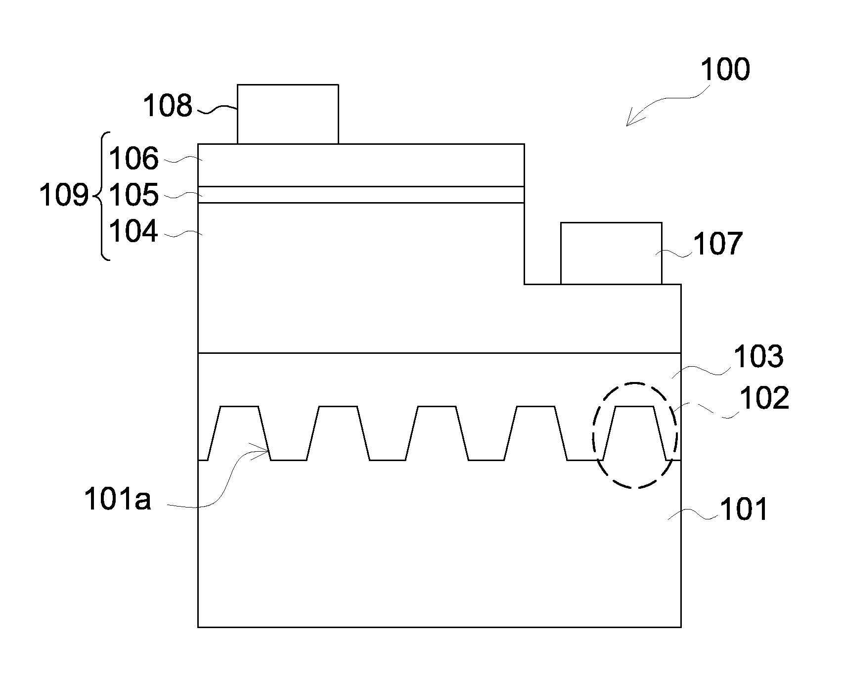
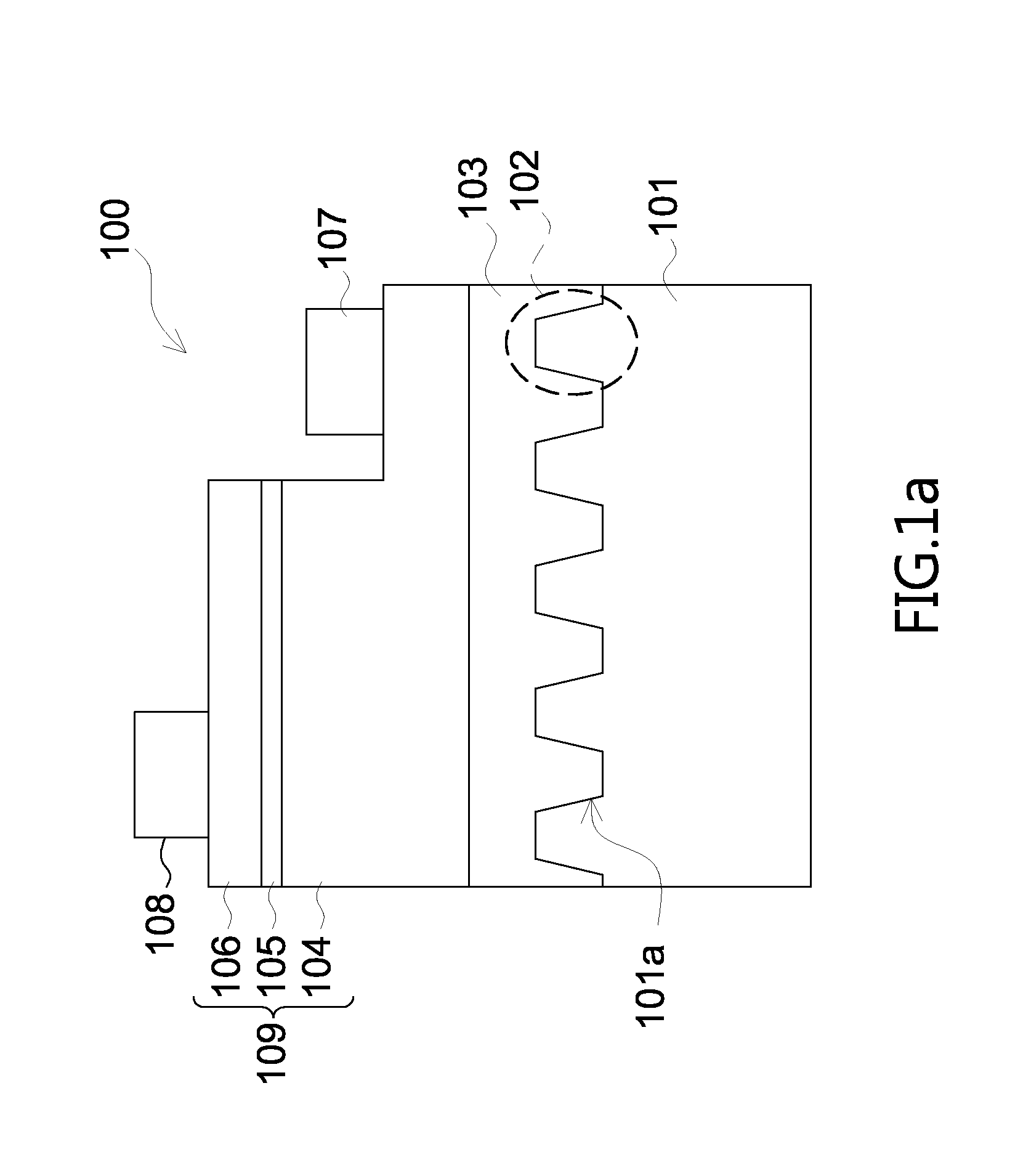
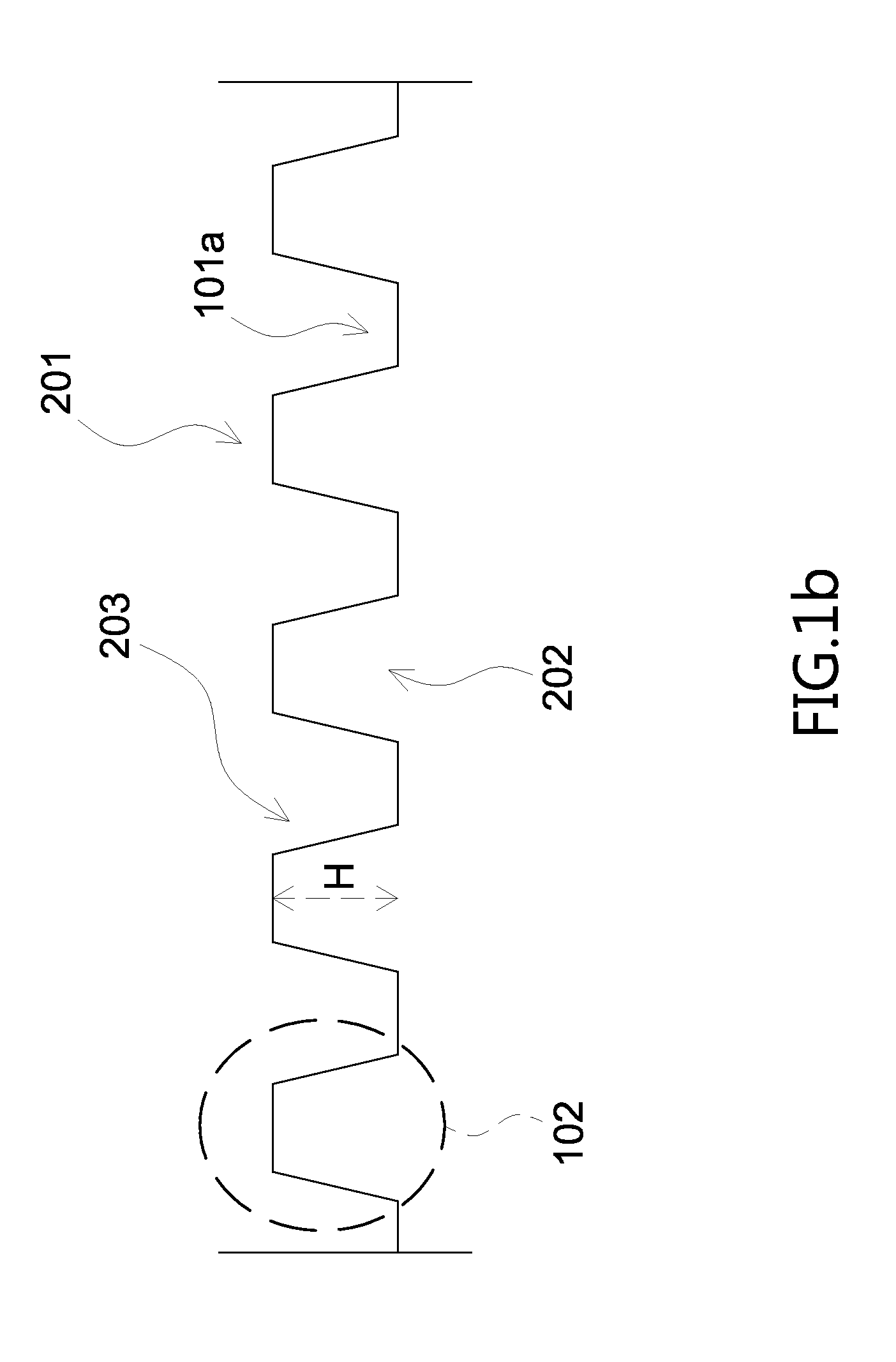
[0014]FIG. 1a shows a light-emitting device (LED) in accordance with one embodiment of the present disclosure. The LED 100 comprises a growth substrate 101, an epitaxial stack 109, a first electrode 107, and a second electrode 108. The cross-section of the substrate 101 shows a plurality of cones 102. In the embodiment, the LED 100 comprises an intermediate layer 103 grown on the substrate 101, and an epitaxial stack 109 grown on the intermediate layer 103.

[0015]The intermediate layer 103 can be a buffer layer used to reduce the lattice mismatch between the substrate 101 and the epitaxial stack 109. The intermediate layer 103 can also be a single layer, multiple layers, or a structure to combine two materials or two separated structures where the material can be organic, inorganic, metal, semiconductor and so on, and the structure can be a reflection layer, a heat conduction layer, an electrical conduction layer, an ohmic contact layer, an anti-deformation layer, a stress release la...


PUM


Abstract

A light-emitting device disclosed herein comprises a patterned substrate having a plurality of cones, wherein a space is between two adjacent cones. A light-emitting stack formed on the cones. Furthermore, the cones comprise an area ratio of a top area of the cone and a bottom area of the cone which is less than 0.0064.

Description

REFERENCE TO RELATED APPLICATION[0001]1. Technical Field[0002]This present application relates to a light-emitting device, and more particularly to a light-emitting device having a patterned substrate and the method of manufacturing.[0003]2. Background of the Disclosure[0004]Recently, efforts have been devoted to improve the luminance of the light-emitting diode (LED) in order to apply the device to the lighting domain, and further procure the goal of energy conservation and carbon reduction. There are two major aspects to improve luminance. One is to increase the internal quantum efficiency (IQE) by improving the epitaxy quality to enhance the combination efficiency of electrons and holes. The other is to increase the light extraction efficiency (LEE) that emphasizes on the light emitted from light-emitting layer and therefore reducing the light absorbed by the LED structure.[0005]Surface roughening technology is one of the efficient methods to enhance luminance, and a well-known m...

Claims


Application Information

Patent Timeline
Patent Type & Authority Applications(United States)
IPC IPC(8): H01L33/24
CPCH01L33/20H01L33/007H01L33/22
Inventor CHANG, CHUNG-YINGWANG, DENNISTSAY, JENQ-DAR
Owner EPISTAR CORP
Why Eureka
Try Eureka