Method for driving liquid crystal display device

a liquid crystal display and display device technology, applied in electronic switching, digital storage, instruments, etc., can solve problems such as degradation of liquid crystal material on the back gate, and achieve the effect of reducing the degradation of liquid crystal material

Active Publication Date: 2014-01-30
SEMICON ENERGY LAB CO LTD
View PDF2 Cites 15 Cited by
  • Summary
  • Abstract
  • Description
  • Claims
  • Application Information

AI Technical Summary

Benefits of technology

[0016]According to one embodiment of the present invention, it is possible to reduce degradation of a liquid crystal material caused by a voltage which is applied to a back gate formed using the same conductive film as a pixel electrode and which controls the shift of the threshold voltage.

Problems solved by technology

The structure disclosed in Patent Document 1, however, has a problem in that a liquid crystal material on the back gate is degraded by a voltage which is applied to the back gate to control the shift of the threshold voltage.

Method used


Image

  • Method for driving liquid crystal display device
  • Method for driving liquid crystal display device
  • Method for driving liquid crystal display device

Examples


embodiment 1

[0033]In this embodiment, one mode of a liquid crystal display device and one mode of a method for driving the liquid crystal display device will be described with reference to FIGS. 1A to 1C, FIGS. 2A and 2B, FIGS. 3A to 3C, FIG. 4, and FIGS. 5A and 5B.

[0034]Before the description of the method for driving the liquid crystal display device according to this embodiment, structures of a pixel circuit and a driver circuit included in the liquid crystal display device will be described.

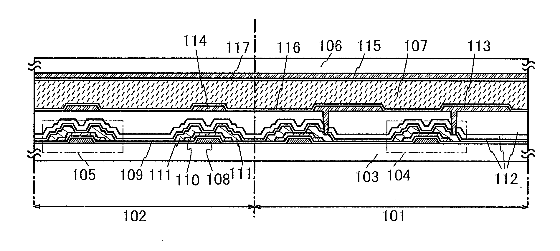
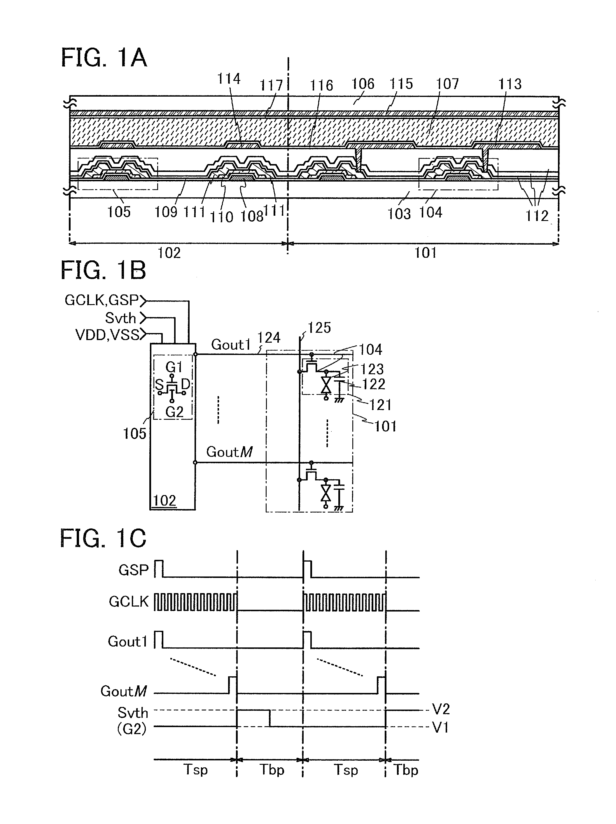
[0035]FIG. 1A is an example of a cross-sectional view of transistors included in a pixel circuit and a driver circuit of the liquid crystal display device.

[0036]In FIG. 1A, a transistor 104 over a substrate 103 is shown in part of a cross-sectional view of a pixel circuit 101, and a transistor 105 over the substrate 103 is shown in part of a cross-sectional view of a driver circuit 102. A substrate 106 is provided so as to face the substrate 103. A liquid crystal layer 107 is provided between the substra...

embodiment 2

[0106]Explained in this embodiment are structures of transistors in the pixel circuit and the driver circuit which are explained in the above Embodiment 1. In this embodiment, detailed description is made on a structure of a so-called bottom-gate transistor, in particular, steps before a conductive film serving as a back gate is provided.

[0107]In a transistor included in the liquid crystal display device shown in the above embodiment, a semiconductor film for forming a channel formation region may be an amorphous, microcrystalline, polycrystalline, or single-crystal semiconductor film of silicon, germanium, or the like, or a semiconductor film of a semiconductor having a wider band gap and lower intrinsic carrier density than silicon. As silicon, any of the following can be used: amorphous silicon formed by a sputtering method or a vapor deposition method such as a plasma CVD method; polycrystalline silicon obtained in such a manner that amorphous silicon is crystallized by laser an...

embodiment 3

[0172]A liquid crystal display device according to one embodiment of the present invention will be described with reference to a block diagram, a schematic view, and a cross-sectional view corresponding to the schematic view of FIGS. 7A to 7C.

[0173]FIG. 7A is a block diagram of a liquid crystal display device. In the liquid crystal display device, a pixel circuit 302, a data line driver circuit 303, and a gate line driver circuit 304 are provided over a substrate 301, and a signal generation circuit 300A and a power source circuit 300B are provided to supply a signal, a power source voltage, and the like necessary for the operation of the driver circuits and the pixel circuit.

[0174]From the signal generation circuit 300A, for example, a data line image signal data, a threshold voltage control signal Svth, a data line start pulse SSP, and a data line clock signal SCLK are output to the data line driver circuit 303. Also from the signal generation circuit 300A, for example, the thresh...


PUM


Abstract

A liquid crystal material is prevented from being degraded by a voltage to control the shift of the threshold voltage which is applied to a back gate on the same conductive film as a pixel electrode. A liquid crystal display device includes a pixel circuit including a pixel electrode which applies an electric field to a liquid crystal layer; and a driver circuit including a transistor including a first gate and a second gate with a semiconductor film interposed therebetween. The transistor overlaps with the liquid crystal layer. A signal for controlling on/off of the transistor is input to the first gate. A signal for applying a first voltage is input to the second gate in a gate line selection period. A signal for alternately applying the first voltage and a second voltage is input to the second gate in a vertical retrace period.

Description

BACKGROUND OF THE INVENTION[0001]1. Field of the Invention[0002]The present invention relates to a liquid crystal display device and a method for driving the liquid crystal display device.[0003]2. Description of the Related Art[0004]Liquid crystal display devices have been commoditized as a result of recent technological innovation, and development thereof has been actively promoted for higher value-added products.[0005]One of the added values for liquid crystal display devices is a reduced frame width around a display area, that is so-called a slim border. The slim border can be achieved in such a manner that transistors in a driver circuit are manufactured over the same substrate as transistors in a pixel circuit in the same process.[0006]For a semiconductor layer of the transistor in the driver circuit, an oxide semiconductor is preferably used because of, for example, easy cost saving due to its productivity which is expected to be as high as that of amorphous silicon. Disclosed...

Claims


Application Information

Patent Timeline
Patent Type & Authority Applications(United States)
IPC IPC(8): G09G3/36
CPCG09G3/36G02F1/1368G09G3/3677G09G2300/0408G09G2300/043G09G2300/0495G11C19/28H03K17/302H03K2217/0018
Inventor YAMAZAKI, SHUNPEIKOYAMA, JUN
Owner SEMICON ENERGY LAB CO LTD
Why Eureka
Try Eureka