
Organic display device and manufacturing method thereof

Inactive Publication Date: 2014-02-06
TCL CHINA STAR OPTOELECTRONICS TECH CO LTD
View PDF5 Cites 2 Cited by
  • Summary
  • Abstract
  • Description
  • Claims
  • Application Information

AI Technical Summary

Benefits of technology

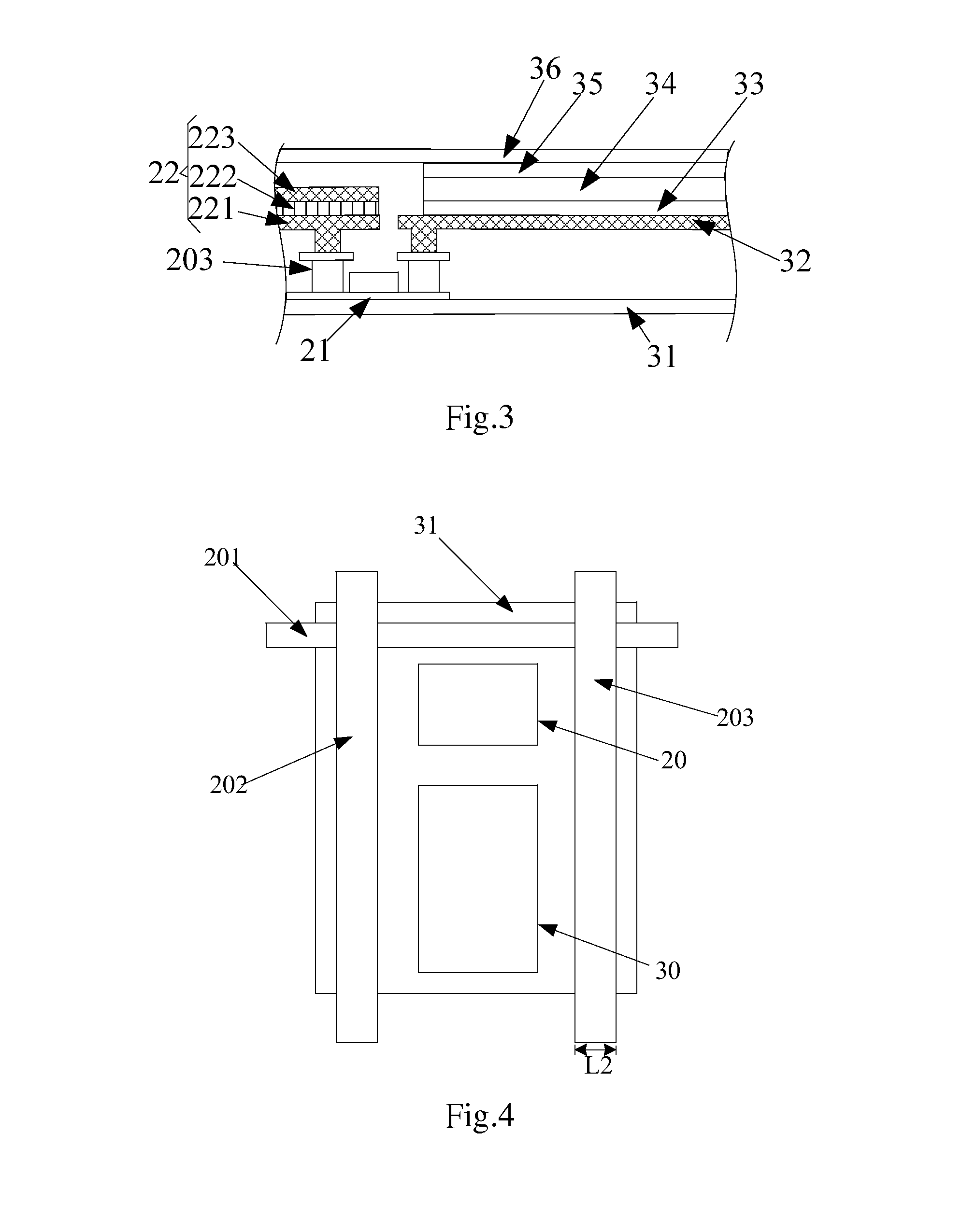
The present invention aims to improve the display quality of organic display devices by reducing the width of power lines and avoiding voltage drops in current transmission. The invention achieves this by using a conductive layer that can function as both a power line and a display region, resulting in a narrower power line width and consistent brightness across the entire display.

Problems solved by technology

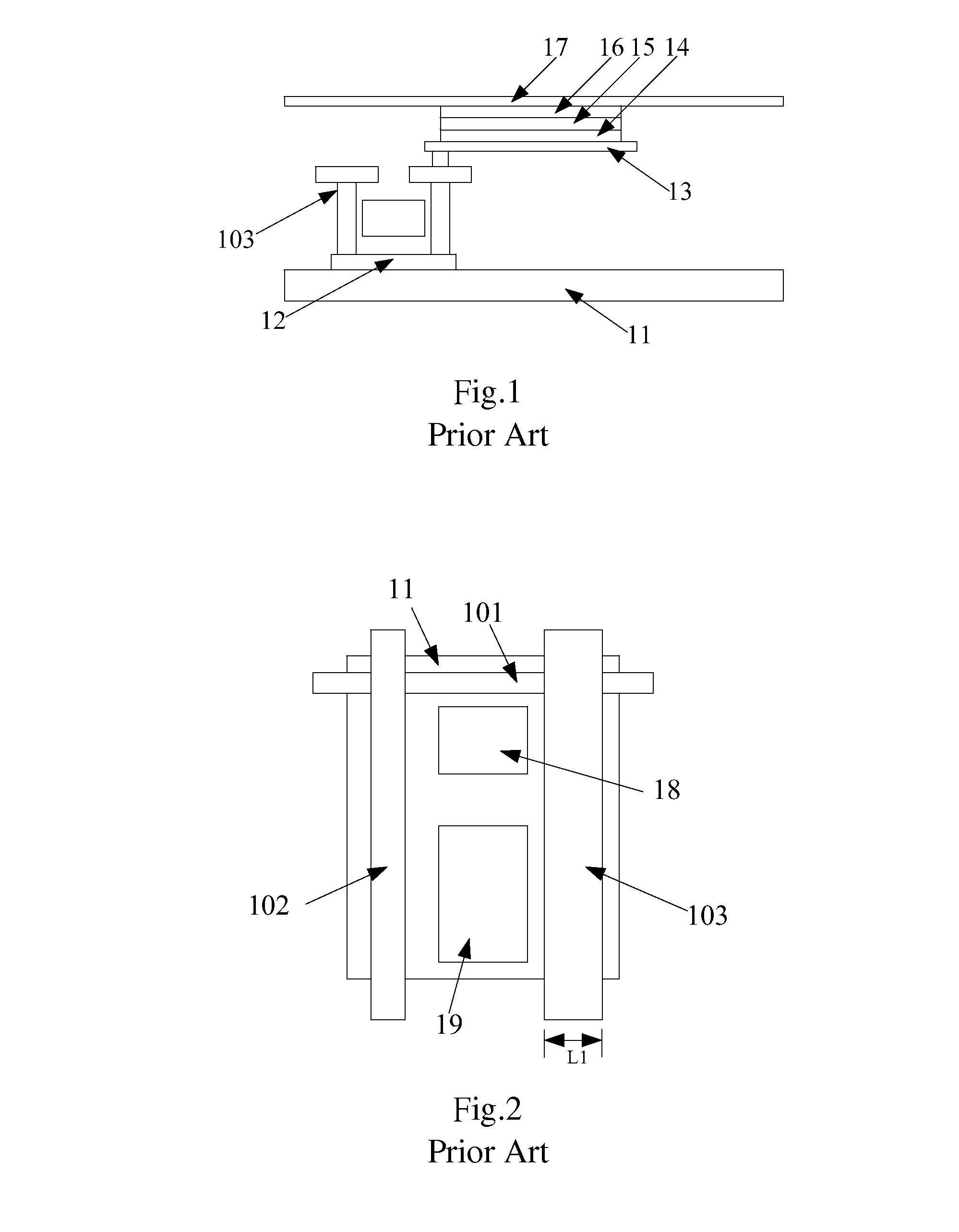
To ensure that the current can be transmitted to each of the organic light emitting diodes, the width L1 of the power lines is generally larger, so that the presence of voltage drops in the transmission process results in different brightness of each of the organic light emitting diodes and thus reduces the display quality.

Method used


Image

  • Organic display device and manufacturing method thereof
  • Organic display device and manufacturing method thereof
  • Organic display device and manufacturing method thereof

Examples


Embodiment Construction

[0044]The following descriptions of the embodiments illustrate the specific implementation of the embodiment according the present invention by referring to the attached drawings. Directional terms described by the present invention, such as upper, lower, front, back, left, right, inner, outer, side, longitudinal / vertical, transverse / horizontal, and etc., are only directions by referring to the accompanying drawings, and thus the used directional terms are used to describe and understand the present invention, but the present invention is not limited thereto. In the figures, the units which have the similar structures are represented by the same numeral.

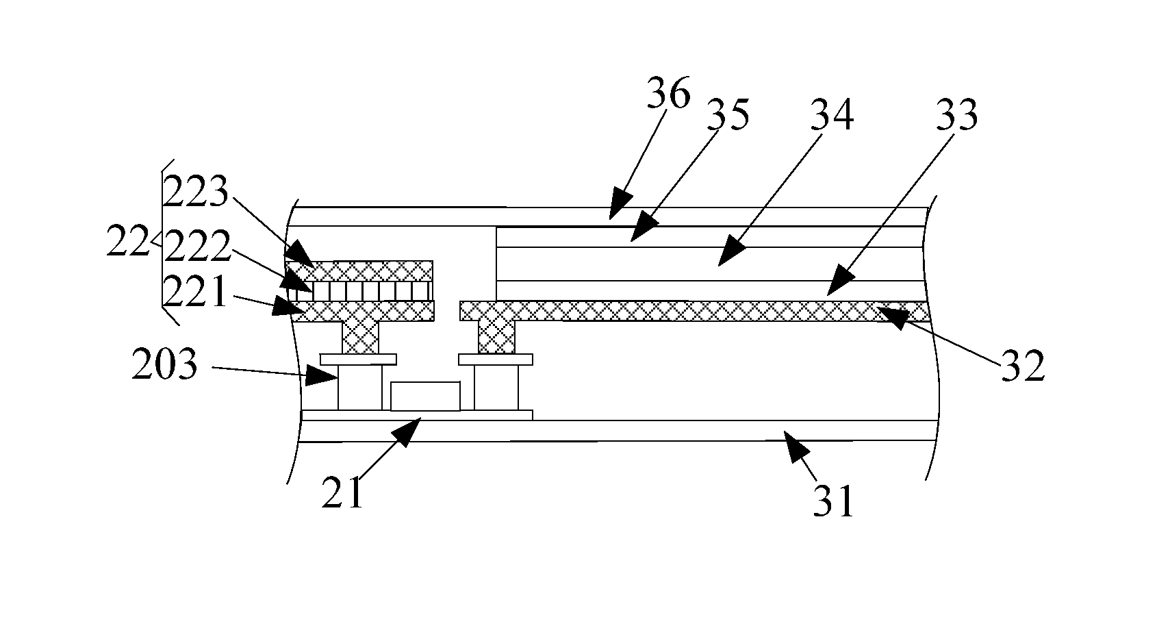
[0045]FIG. 4 is a top structural view of the organic display device according to a preferred embodiment of the present invention. The organic display device comprises data lines 201, scan lines 202, and power lines 203, which are formed on the same layer by the same manufacturing process. The portions crossed and defined by the data ...


PUM


Abstract

An organic display device and a method of manufacturing method thereof are provided. The organic display device includes scan lines, data lines and power lines. Portions crossed and defined by the scan lines, the data lines and the power supply lines are provide with display regions. The display region is formed with an organic light emitting diode. The organic light emitting diode includes an anode layer, and a conductive layer is formed on the power supply line. The anode layer of the organic light emitting diode and the conductive layer are etched and formed on the same basis of a material layer.

Description

FIELD OF THE INVENTION[0001]The present invention relates to a field of display technology, and more particularly to an organic display device and a manufacturing method thereof.BACKGROUND OF THE INVENTION[0002]The organic electroluminesence display (OELD) is a new generation of display device which generally adapts organic light emitting diodes (OLED) as light-emitting display components.[0003]The organic light emitting diodes emit light by sandwiching the organic light-emitting material between the transparent anode and the metal reflecting cathode and applying a voltage to the organic light-emitting material. Because the organic electroluminesence displays do not require the liquid crystals and the conventional backlight modules, they can be manufactured thinner. Compared with other type of flat display devices, the OLEDs consume less power, work in the wider range of temperatures and cost lower, and therefore they are used more and more widely.[0004]Please referring to FIG. 1, F...

Claims


Application Information

Patent Timeline
IPC IPC(8): H01L27/32H01L51/56
CPCH01L51/56H01L27/32H10K59/1315H10K71/00H10K59/80516H10K71/233H10K59/00
Inventor HWANG, TAI-JIUN
Owner TCL CHINA STAR OPTOELECTRONICS TECH CO LTD
Learn More