Liquid crystal device and electronics apparatus

Active Publication Date: 2007-10-04
JAPAN DISPLAY WEST
View PDF12 Cites 50 Cited by
  • Summary
  • Abstract
  • Description
  • Claims
  • Application Information

AI Technical Summary

Benefits of technology

[0013]An advantage of some aspects of the invention is that it provides a liquid crystal device in FFS mode having a pixel structur

Problems solved by technology

Liquid crystal molecules located above the pixel electrodes are not sufficiently driven, resulting in a reduction in transmittance or the like.
This results in a generation of a domain region where liquid crystal

Method used


Image

  • Liquid crystal device and electronics apparatus
  • Liquid crystal device and electronics apparatus
  • Liquid crystal device and electronics apparatus

Examples


Example

First Embodiment

Structure of Liquid Crystal Device

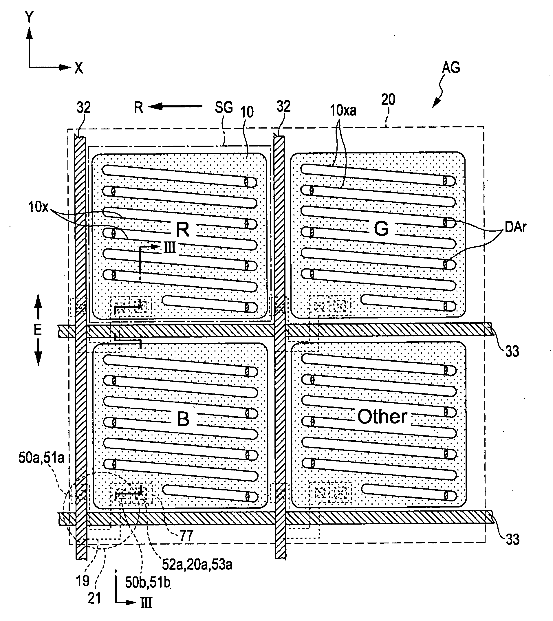
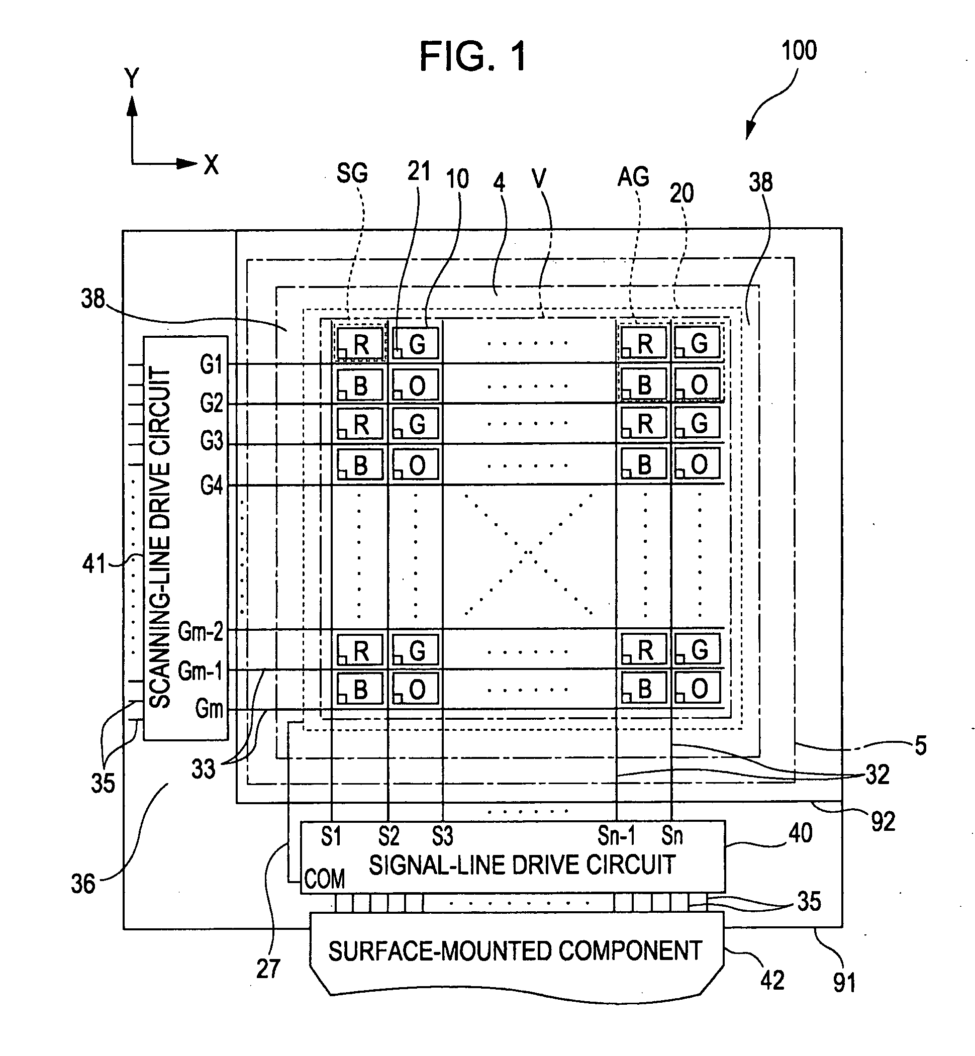
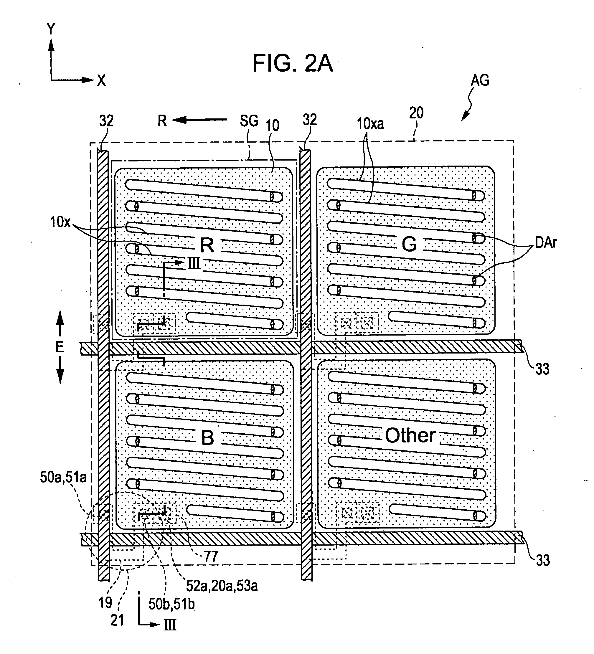
[0045]With reference to FIG. 1 and the like, the structure of a liquid crystal device 100 and the like according to a first embodiment of the invention will be described.

[0046]FIG. 1 is a plan view schematically showing the schematic structure of the liquid crystal device 100 according to the first embodiment of the invention. In FIG. 1, a color filter substrate 92 is placed at the front side when viewed in FIG. 1(near the observer of FIG. 1), and an element substrate 91 is placed at the rear side when viewed in FIG. 1. The vertical direction in FIG. 1 (column direction, which is the direction in which columns extend) is defined as the Y-direction, and the horizontal direction in FIG. 1 (row direction, which is the direction in which rows extend) is defined as the X-direction. In FIG. 1, regions represented by red (R), green (G), blue (B), and an arbitrary color (other, which may be abbreviated as “O”) indicate subpixel regions SG, a...

Example

Second Embodiment

[0131]With reference to FIGS. 2B and 4, a liquid crystal device 200 according to a second embodiment of the invention will be described.

[0132]FIG. 2B shows the planar structure of one pixel of an element substrate 93 according to the second embodiment. In FIG. 2B, only the minimum components necessary for describing the element substrate 93 are shown. FIG. 4 is a cross-sectional view, taken along the line IV-IV of FIG. 2B, of one subpixel cut at the position across the LTPS TFT 21.

[0133]When the second embodiment is compared with the first embodiment, the main difference is that the positional relationship between the common electrode 20 and the pixel electrodes 10 with respect to the third insulating film 53 serving as a dielectric film on the element substrate is reversed, and the other structural portions are common in both embodiments. Therefore, components common to those in the first embodiment are denoted by the same reference numerals, and descriptions there...


PUM


Abstract

A liquid crystal device includes a substrate having unit pixels, each of which includes a plurality of subpixels arranged in a plurality of rows and a plurality of columns. The substrate includes switching elements, a first insulating film disposed at least on the switching elements, a first transparent electrode disposed on the first insulating film, a second transparent electrode disposed on the second insulating film, having a plurality of slits corresponding to each one of the subpixels, and generating an electric field through the slits between the first and second transparent electrodes. The direction in which a long side of each of the slits extends is defined to be different from the direction in which the columns extend.

Description

BACKGROUND[0001]1. Technical Field[0002]The present invention relates to liquid crystal devices for use in displaying various types of information and to electronic apparatuses.[0003]2. Related Art[0004]Generally, liquid crystal display modes can be classified into the following three types: twisted nematic (TN) mode; vertical alignment mode intended to increase the viewing angle and contrast; and transverse electric field mode represented by in-plane switching (IPS) mode or fringe field switching (FFS) mode.[0005]Among these modes, IPS mode is a mode in which the direction of electric field applied to liquid crystal is substantially parallel to a substrate. IPS mode is advantageous over TN mode or the like in that IPS mode can improve viewing angle characteristics.[0006]However, in such a liquid crystal device, pixel electrodes made of a transparent conductive material such as indium tin oxide (ITO) or the like and a common electrode for generating a transverse electric field betwe...

Claims


Application Information

Patent Timeline
IPC IPC(8): G02F1/1343
CPCG02F1/133707G02F1/134363G02F2202/104G02F2001/134372G02F2201/52G02F2001/134345G02F1/134345G02F1/134372G02F1/1343
Inventor FUJITA, SHIN
Owner JAPAN DISPLAY WEST
Why Eureka
Try Eureka