This helps you quickly interpret patents by identifying the three key elements:
Problems solved by technology
Method used
Benefits of technology
Benefits of technology
The patent describes a new design for a partition used in electronic devices. The partition is made up of different materials that have a curved surface on the lower layer and a flat surface on the upper layer. This design reduces the depth of the partition and prevents light leakage and viewing angle dependency, resulting in improved contrast and reduced leakage current.
Problems solved by technology
On the other hands, as the position of the viewer's eye deviates from the direction perpendicular to the panel plane, it becomes difficult for the viewer to recognize light of the desired color.
Further, as the height of a partition separating pixels becomes larger, that is, the distance between a top surface of a reflective electrode and a color filter becomes larger, viewing angle dependency increases.
The viewing angle dependency becomes a big issue, particularly in a large-sized panel.
Method used
Image
Click on the blue label to locate the original text in one second.
Reading with bidirectional positioning of images and text.
Examples
embodiment 1
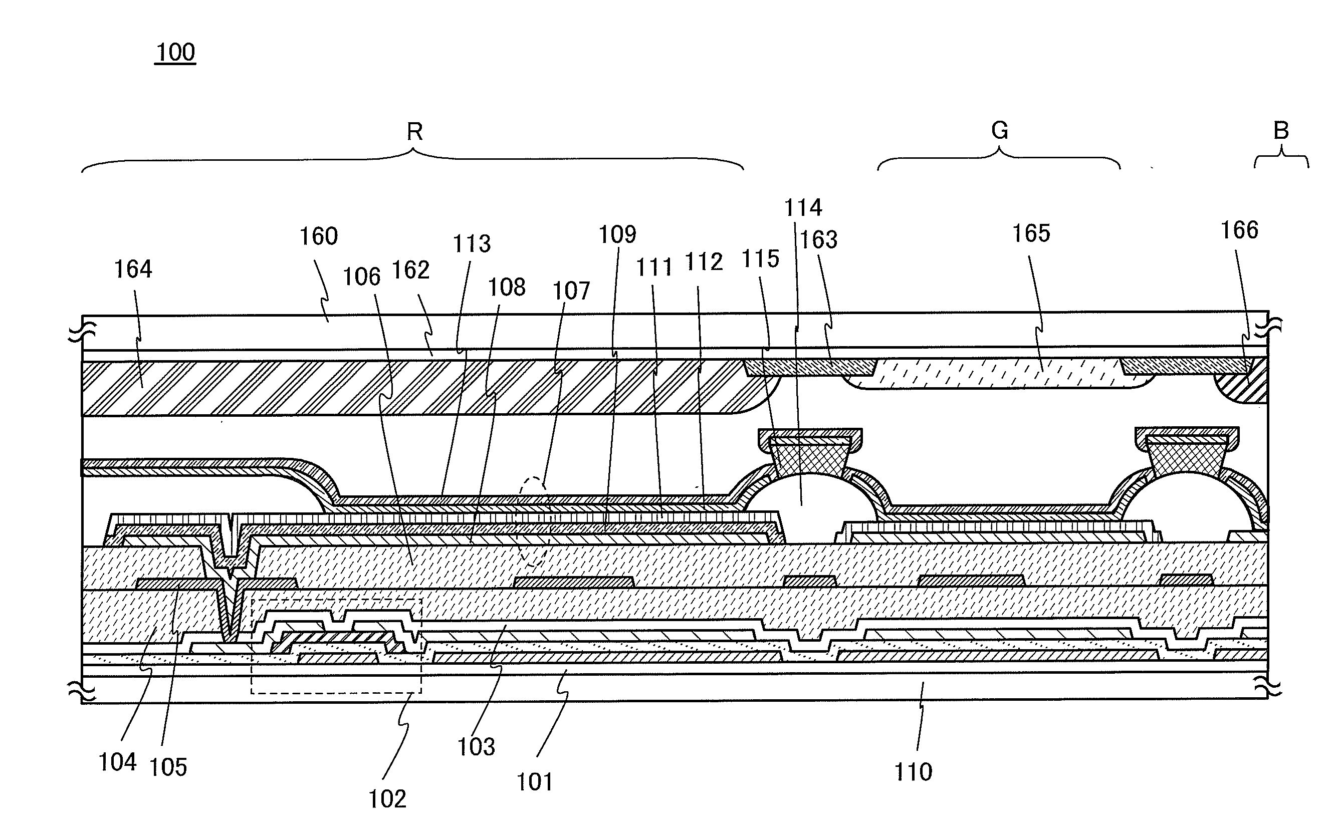
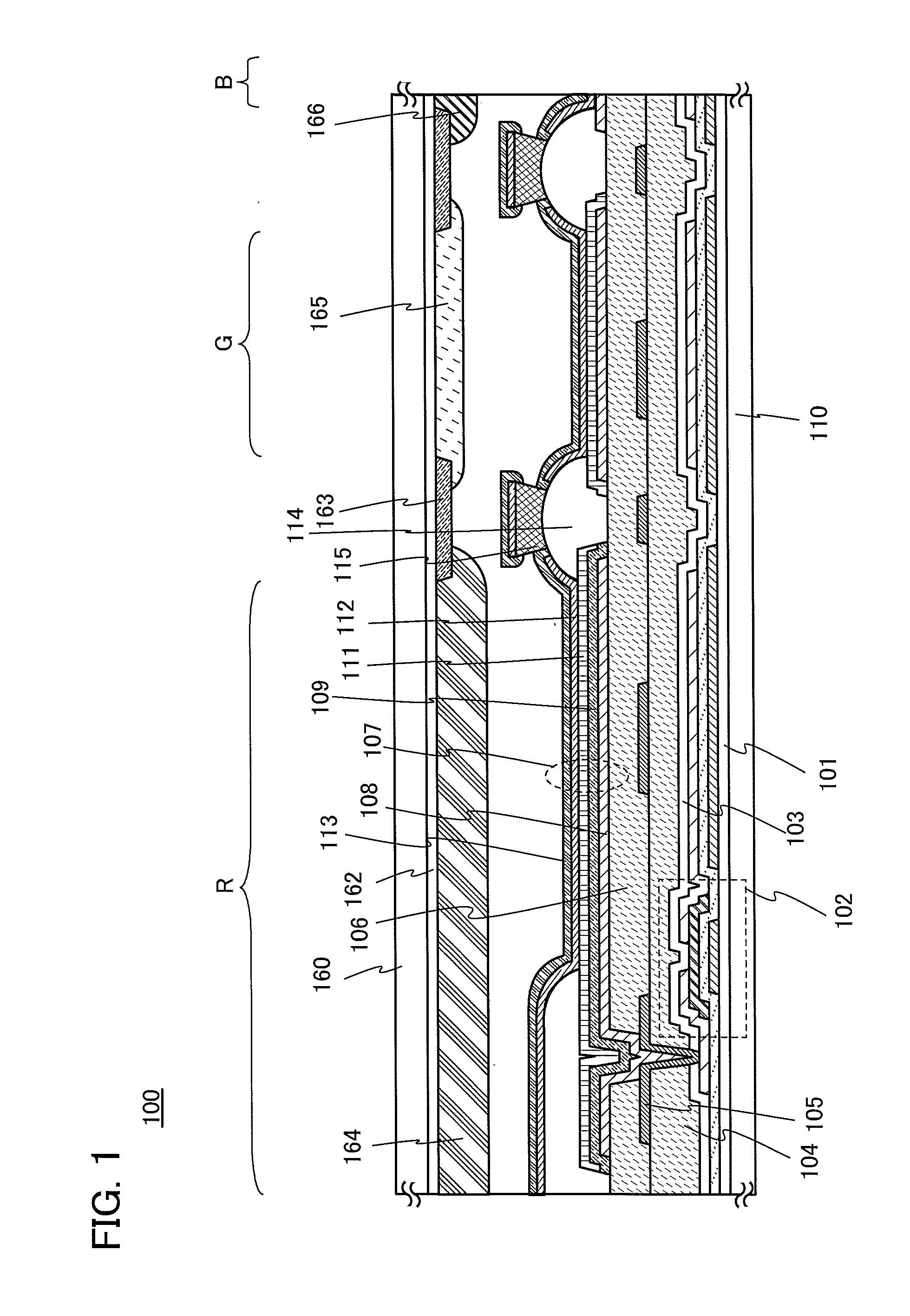
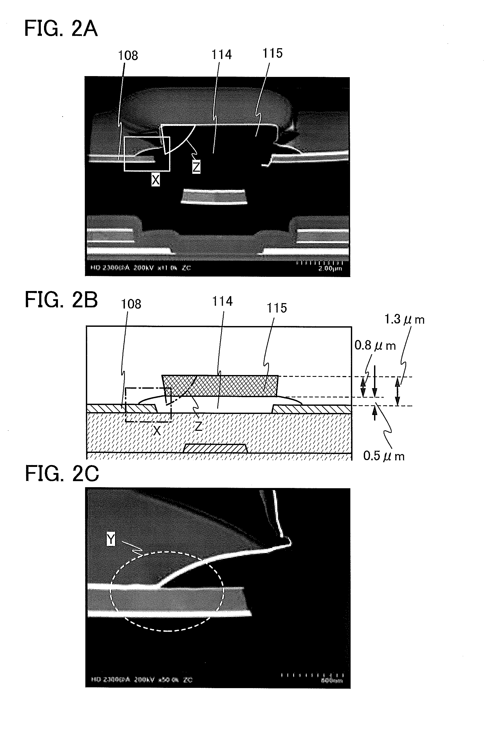
[0064]In this embodiment, an organic EL display device which achieves high-definition display will be described. In the organic EL display device, a shape of a partition is adjusted, and the height of the partition is controlled to be greater than or equal to 0.5 μm and less than or equal to 1.3 μm.
[0065]FIG. 1 is a cross-sectional view illustrating a specific structure of an organic EL display device 100. In the structure illustrated in FIG. 1, a wiring layer is formed between a light-emitting element and a transistor. Thus, even when the number of transistors included in each pixel is increased in accordance with high-definition display, the pixel can be miniaturized.
[0066]As illustrated in FIG. 1, the organic EL display device 100 includes a first substrate 110, a base layer 101 over the first substrate 110, a transistor 102 and an insulating layer 103 over the base layer 101, a first interlayer film 104 over the insulating layer 103, a wiring 105 electrically connected to the tr...
embodiment 2
[0202]In this embodiment, an organic EL display device 200 which enables high-definition display will be described. In the organic EL display device 200, a shape of a partition is adjusted, and the height of the partition is controlled to be higher than or equal to 0.5 μm and less than or equal to 1.3 μm.
[0203]Note that except that a wiring layer is not formed between a light-emitting layer and a transistor, the organic EL display device 200 described in this embodiment can have a structure similar to that of the organic EL display device 100 described in Embodiment 1. Thus, Embodiment 1 can be referred to for the detailed description.
[0204]As illustrated in FIG. 8, the organic EL display device 200 includes a first substrate 240, a base layer 204 over the first substrate 240, a transistor 250 over the base layer 204, an insulating layer 214, a first interlayer film 216 over the insulating layer 214, a light-emitting element 230 electrically connected to the transistor 250, and a fi...
PUM
Abstract
To improve image quality of a full-color organic EL display panel. A partition has a stacked structure formed using different materials. A lower partition has a curved shape, and an upper partition has a flat top surface. An angle formed between a plane surface connecting a lower end of a side surface with an upper end of the side surface of the upper partition and the top surface of the upper partition is less than or equal to 90°. The height of the partition is controlled to be greater than or equal to 0.5 μm and less than or equal to 1.3 μm. With such a structure, a large color organic EL display panel achieves high-definition display.
Description
BACKGROUND OF THE INVENTION[0001]1. Field of the Invention[0002]The present invention relates to a display device and a method for manufacturing the display device. In particular, the present invention relates to a display device utilizing organic electroluminescence (EL) (the device is referred to as organic EL display device) and a method for manufacturing the display device.[0003]The present invention relates to an organic EL display device including a high-definition display panel and a method for manufacturing the organic EL display device. In particular, the present invention relates to an organic EL display device in which a shape of a partition separating pixels and a height of the partition are adjusted, and a method for manufacturing the organic EL display device.[0004]2. Description of the Related Art[0005]In recent years, color organic EL display panels using an oxidesemiconductor for a TFT have been suggested. Varied development has been conducted. For example, in orde...
Claims
Application Information
Patent Timeline
Application Date:The date an application was filed.
Publication Date:The date a patent or application was officially published.
First Publication Date:The earliest publication date of a patent with the same application number.
Issue Date:Publication date of the patent grant document.
PCT Entry Date:The Entry date of PCT National Phase.
Estimated Expiry Date:The statutory expiry date of a patent right according to the Patent Law, and it is the longest term of protection that the patent right can achieve without the termination of the patent right due to other reasons(Term extension factor has been taken into account ).
Invalid Date:Actual expiry date is based on effective date or publication date of legal transaction data of invalid patent.

