
Image processing apparatus, display system, electronic apparatus, and method of processing image

a technology of image processing and electronic equipment, applied in the field of image processing equipment, display systems, electronic equipment, image processing methods, can solve the problems of reducing the product yield, affecting the product quality, so as to reduce the information amount of correction information

Active Publication Date: 2015-05-12
SEIKO EPSON CORP
View PDF56 Cites 0 Cited by
  • Summary
  • Abstract
  • Description
  • Claims
  • Application Information

AI Technical Summary

Benefits of technology

The patent describes a way to adjust the brightness and color of LED displays by using information about the current that drives them. This helps to correct any variations in LED performance and ensure consistent brightness and color across the entire display. By measuring the difference between the current of adjacent pixels, the system can generate precise correction information with minimal data needed. This approach reduces the amount of data needed to be stored and transmitted, making it more efficient and reliable.

Problems solved by technology

However, in the display panel using the OLED's, as a differing organic material is used for each color component configuring one pixel, a difference occurs in the degree of degradation in luminance after use, causing a deterioration in image quality.
Also, with the display panel using the OLED's, a luminance and color unevenness attributed to manufacture reduces a product yield, which also becomes a factor in preventing a reduction in cost.
However, the luminance and color unevenness are caused by a variation in light emitting elements themselves and a variation in a drive current which drives the light emitting elements.
For this reason, with the technologies disclosed in Patent Document 1 and Patent Document 2, it is not possible to simultaneously correct the variation in the light emitting elements and the variation in the drive current which drives the light emitting elements, and it is not possible to reduce the luminance and color unevenness of the display panel using the OLED's with a high precision.

Method used


Image

  • Image processing apparatus, display system, electronic apparatus, and method of processing image
  • Image processing apparatus, display system, electronic apparatus, and method of processing image
  • Image processing apparatus, display system, electronic apparatus, and method of processing image

Examples


Embodiment Construction

[0048]Hereafter, a detailed description will be given, using the drawings, of an embodiment of the invention. The embodiment, to be described hereafter, does not unduly limit the details of the invention described in the claims. Also, not all of configurations to be described hereafter are constituent features essential for solving the problems of the invention.

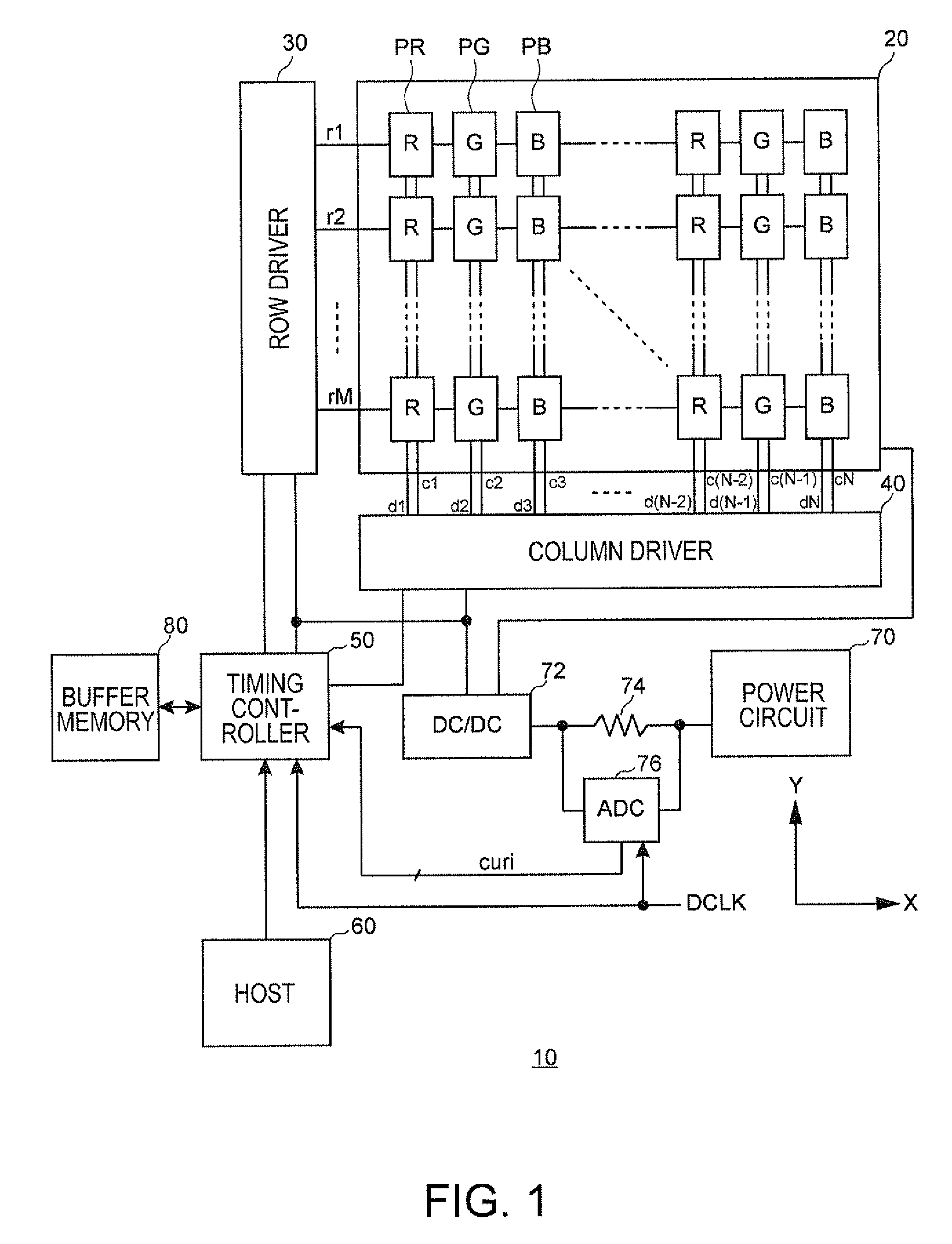
[0049]FIG. 1 shows a block diagram of a configuration example of a display system according to the embodiment of the invention. The display system has a display panel (a light emitting panel) using OLED's which are light emitting elements acting as display elements, and each OLED is driven by a row driver and a column driver based on a display timing control signal generated by a timing controller.

[0050]More specifically, the display system 10 includes a display panel 20, a row driver 30, a column driver 40, a timing controller 50 (in the broad sense, an image processing circuit or an image processing apparatus), a host 60, a...


PUM


Abstract

An image processing apparatus which corrects pixel data corresponding to pixels configuring a display image of a display device having light emitting elements includes an information storage unit which, in units of one or a plurality of pixels of the display device, stores information corresponding to operating currents of light emitting elements included in the one or plurality of pixels, and a pixel data correction unit which corrects the pixel data based on the information corresponding to the operating currents stored in the information storage unit.

Description

[0001]This application claims priority based on Japanese Patent Application No. 2009-195123, filed on Aug. 26, 2009, which is incorporated in this specification.BACKGROUND[0002]1. Technical Field[0003]An aspect of the present invention relates to an image processing apparatus, a display system, an electronic apparatus, an image processing method.[0004]2. Background Art[0005]In recent years, an LCD (liquid crystal display) panel using liquid crystal elements as display elements, and a display panel (a display device) using organic light emitting diodes (hereafter abbreviated as OLED's) (in the broad sense, light emitting elements) as display elements, have been in widespread use. In particular, OLED's having a high response speed, it is possible to improve a contrast ratio. For this reason, according to a display panel having OLED's disposed in a matrix form, it is possible to display a high quality image with a wide viewing angle.[0006]However, in the display panel using the OLED's,...

Claims


Application Information

Patent Timeline
Patent Type & Authority Patents(United States)
IPC IPC(8): G09G3/30G09G3/32
CPCG09G3/3233G09G2320/0285G09G2320/029G09G2320/043
Inventor KIKUTA, KAZUTO
Owner SEIKO EPSON CORP
Learn More