Latch-up suppression and substrate noise coupling reduction through a substrate back-tie for 3D integrated circuits

Active Publication Date: 2014-03-06
SYNOPSYS INC
View PDF3 Cites 9 Cited by
  • Summary
  • Abstract
  • Description
  • Claims
  • Application Information

AI Technical Summary

Benefits of technology

The patent describes a type of integrated circuit with a conductor that runs all the way through the device. This conductor is insulated from other conductors and other parts of the device, which makes it easier to control and reduces interference. This design can be useful in creating complex integrated circuits that are more efficient and reliable.

Problems solved by technology

When this occurs, a positive feedback loop ensues which provides a low resistance current path from the positive supply voltage to ground, thereby interfering with proper functioning of the circuit and, in serious cases, destroying the chip through heat damage.
A number of conditions can trigger latch-up however, including noise, which sometimes can induce sufficient current at the base of one of the transistors for long enough to forward bias the other transistor, thereby starting a feedback loop.
3DIC technology poses a number of problems for known techniques for suppressing latch-up.
First, because of the difficulties in fabricating very deep TSVs, chip substrates used in 3DICs typically are considerably thinned, from the backside, to a thickness of only around 50 microns.
Moreover, down-bonding is no longer available to short circuit this current path, since the substrate backside is not connected by die attach adhesive to a below-adjacent lead frame pad.

Method used


Image

  • Latch-up suppression and substrate noise coupling reduction through a substrate back-tie for 3D integrated circuits
  • Latch-up suppression and substrate noise coupling reduction through a substrate back-tie for 3D integrated circuits
  • Latch-up suppression and substrate noise coupling reduction through a substrate back-tie for 3D integrated circuits

Examples


Embodiment Construction

[0025]The following description is presented to enable any person skilled in the art to make and use the invention, and is provided in the context of a particular application and its requirements. Various modifications to the disclosed embodiments will be readily apparent to those skilled in the art, and the general principles defined herein may be applied to other embodiments and applications without departing from the spirit and scope of the present invention. Thus, the present invention is not intended to be limited to the embodiments shown, but is to be accorded the widest scope consistent with the principles and features disclosed herein.

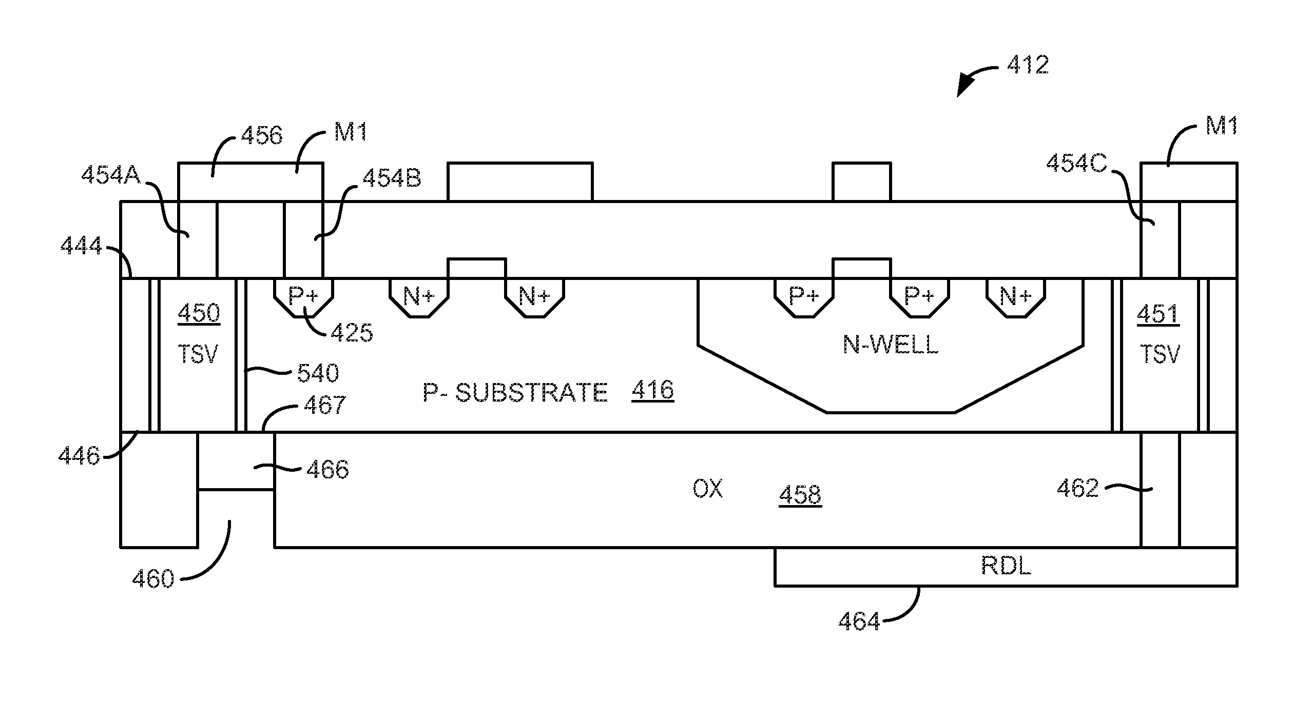
[0026]FIG. 4 is a cross-sectional view illustrating pertinent features of a 3D integrated circuit structure 410 incorporating aspects of the invention. The drawing, as with all drawings herein, is not to scale. Only a small part of the structure is shown, and it will be understood that typically each chip is much larger (laterally) and includes...


PUM


Abstract

Roughly described, an integrated circuit device has a conductor extending entirely through the substrate, connected on one end to the substrate topside surface and on the other end to the substrate backside surface. In various embodiments the conductor is insulated from all RDL conductors on the backside of the substrate, and / or is insulated from all conductors and device features on any below-adjacent chip in a 3D integrated circuit structure. Methods of fabrication are also described.

Description

BACKGROUND[0001]The invention relates to 3D integrated circuits, and more particularly to structures and methods for suppressing latch-up and noise coupling.[0002]A typical CMOS circuit includes N- and P-type regions arranged to form planar or multi-gate MOS transistors. Regions of opposite conductivity types which are adjacent each other typically form parasitic pn junctions and bipolar transistor structures. While usually reverse-biased, conditions can occur in which these structures become forward biased. When this occurs, a positive feedback loop ensues which provides a low resistance current path from the positive supply voltage to ground, thereby interfering with proper functioning of the circuit and, in serious cases, destroying the chip through heat damage.[0003]FIG. 1 is a schematic diagram showing a typical CMOS arrangement including a PMOS transistor 110 adjacent to an NMOS transistor 112. Such proximity is common in CMOS devices. The PMOS transistor 110 includes two heav...

Claims


Application Information

Patent Timeline
IPC IPC(8): H01L21/768G06F17/50H01L23/48
CPCH01L23/481H01L21/768H01L21/76898H01L23/48H01L24/05H01L24/13H01L2224/02372H01L2224/0401H01L2224/05H01L2224/05548H01L2224/13024H01L2224/16238H01L2924/1305H01L2924/13091
Inventor MOROZ, VICTORKAWA, JAMIL
Owner SYNOPSYS INC
Why Eureka
Try Eureka