
Pre-Molded MEMS Device Package

a technology for mems devices and packaging, applied in the field of mems devices, can solve the problems of moving parts being damaged or fixed in place, and the packaging and packaging are not suitable for all devices

Active Publication Date: 2014-03-13
INVENSENSE
View PDF5 Cites 11 Cited by
  • Summary
  • Abstract
  • Description
  • Claims
  • Application Information

AI Technical Summary

Benefits of technology

The patent describes a package for a MEMS device, such as a microphone, that includes a lead frame, a mold body, and a conductive cover. The lead frame has a die-bonding area and a connector surface, and the mold body partially encapsulates the lead frame. The conductive cover is physically and electrically coupled to the lead frame and the mold body, forming an enclosed chamber within the package. The package also includes conductive bumps and through mold vias for connecting to a circuit board. The technical effects of this package include improved protection and reliability of the MEMS device, reduced size and weight, and improved performance and reliability of the package.

Problems solved by technology

Such techniques and packages are not suitable for all devices, however.
Such moving parts may be damaged or fixed in place by the injected plastic, for example.

Method used


Image

  • Pre-Molded MEMS Device Package
  • Pre-Molded MEMS Device Package
  • Pre-Molded MEMS Device Package

Examples


first embodiment

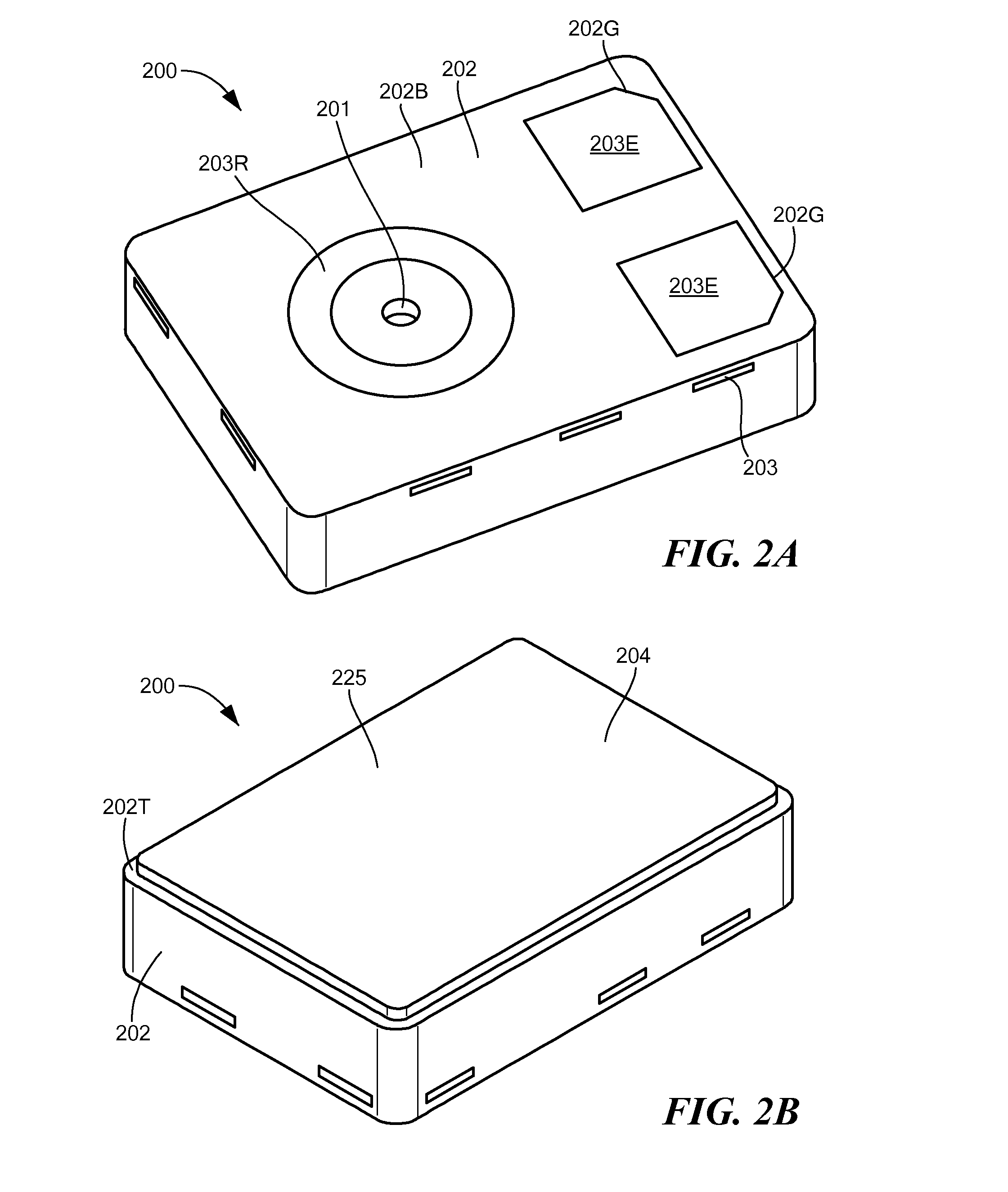
[0006]In the invention, there is provided a package for a MEMS device, the package including a lead frame comprising a die-bonding area, and a plurality of bond pads; a mold body forming a cavity and an exterior surface, the mold body partially encapsulating the lead frame and having an interior window area to accommodate the die-bonding area and exterior window area in the bottom surface to accommodate the plurality of bond pads; a MEMS device mounted in the cavity; a conductive cover, the conductive cover physically coupled to the mold body and completely covering the cavity so as to form an enclosed chamber within the package, the MEMS device contained within the chamber; and a conductive column, the conductive column comprising a hole within the mold body and an electrically conductive material within the hole, the electrically conductive material electrically and physically coupled to the lead frame and to the cover.

[0007]In another embodiment, the package includes a plurality ...

embodiment 800

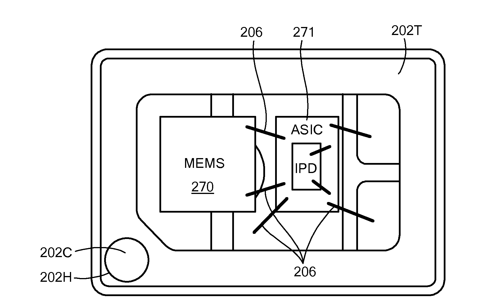
[0078]Some embodiments include a partial shell within the package to provide additional EMI protection. FIG. 8A-8E schematically illustrate various portions of one embodiment 800, including mold body 202 and lead frame 203, which are fabricated in accordance with the methods described above.

[0079]Package 800 also includes a half-shell, or tub, 810 within cavity 205. The shell 810 may, in some embodiments, have a shape similar to the shape of a bathtub. In some embodiments, the shell 801 may include a flange 813 about its periphery to support the shell within a mold body (see, for example, FIG. 8B), and / or to provide a surface for making contact with a cover. In some embodiments, shell 810 may have shoulders and surfaces to support integrated circuit 271 spaced from MEMS device 270, similar to the shoulders 706 and surfaces 706A described above. In some embodiments, the shell 810 has a shape that matches the contour of the cavity in the mold body.

[0080]Shell 810 is conductive, and ma...


PUM


Abstract

A MEMS lead frame package body encloses a MEMS device enclosed in an internal cavity formed by the mold body and cover. To accommodate a MEMS microphone, an acoustic aperture extends through the mold body. In some embodiments, a conductive column extends through the pre-molded body to allow electrical connection from a partially encapsulated lead frame to the conductive cover. Some embodiments may include a multi-tiered cavity within the mold body for mounting an integrated circuit separated by a gap above the MEMS device.

Description

[0001]This application claims priority to U.S. Provisional Patent Application No. 61 / 698,966 filed Sep. 10, 2012, the full disclosure of which is hereby incorporated by reference herein.[0002]Related application filed on the same date as the present application and having the same inventor and same assignee as the present application, entitled “Pre-Molded MEMS Device Package With Conductive Shell” and bearing attorney docket number 2550 / E40 is hereby incorporated by reference herein in its entirety.TECHNICAL FIELD[0003]The present invention relates to MEMS devices, and particularly to packaging for MEMS devices.BACKGROUND ART[0004]It is known in the prior art to package integrated circuits in any of a variety of plastic packages. Some plastic packages involve mounting an integrated circuit to a lead frame, and then placing the integrated circuit, and portions of the lead frame, within a mold, and filling the mold with fluid plastic. When the plastic hardens, the integrated circuit a...

Claims


Application Information

Patent Timeline
IPC IPC(8): B81B7/00
CPCB81B7/0032H01L2224/48137H01L2224/48247H01L2924/19011H01L2924/19104H01L2924/3025B81B7/0077H01L2924/1461H01L2924/00H01L21/50H01L23/495B81B7/007B81B2201/0257B81B2207/093
Inventor GOIDA, THOMAS M.
Owner INVENSENSE
Learn More