Color filter substrate, method of fabricating the same, and LCD panel
a technology of color filter substrate and lcd panel, which is applied in the manufacture of cables/conductor parts, instruments, optics, etc., can solve the problems of lcd panel, and achieve the effect of improving the transparency of lcd panel, increasing the magnitude of electric field, and maximising transmittan
- Summary
- Abstract
- Description
- Claims
- Application Information
AI Technical Summary
Benefits of technology
Problems solved by technology
Method used
Image
Examples
embodiment 1
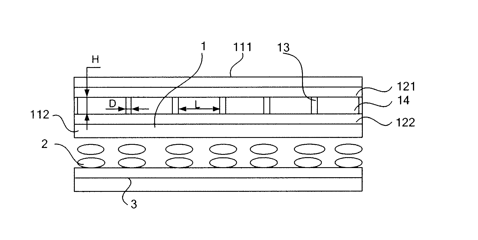
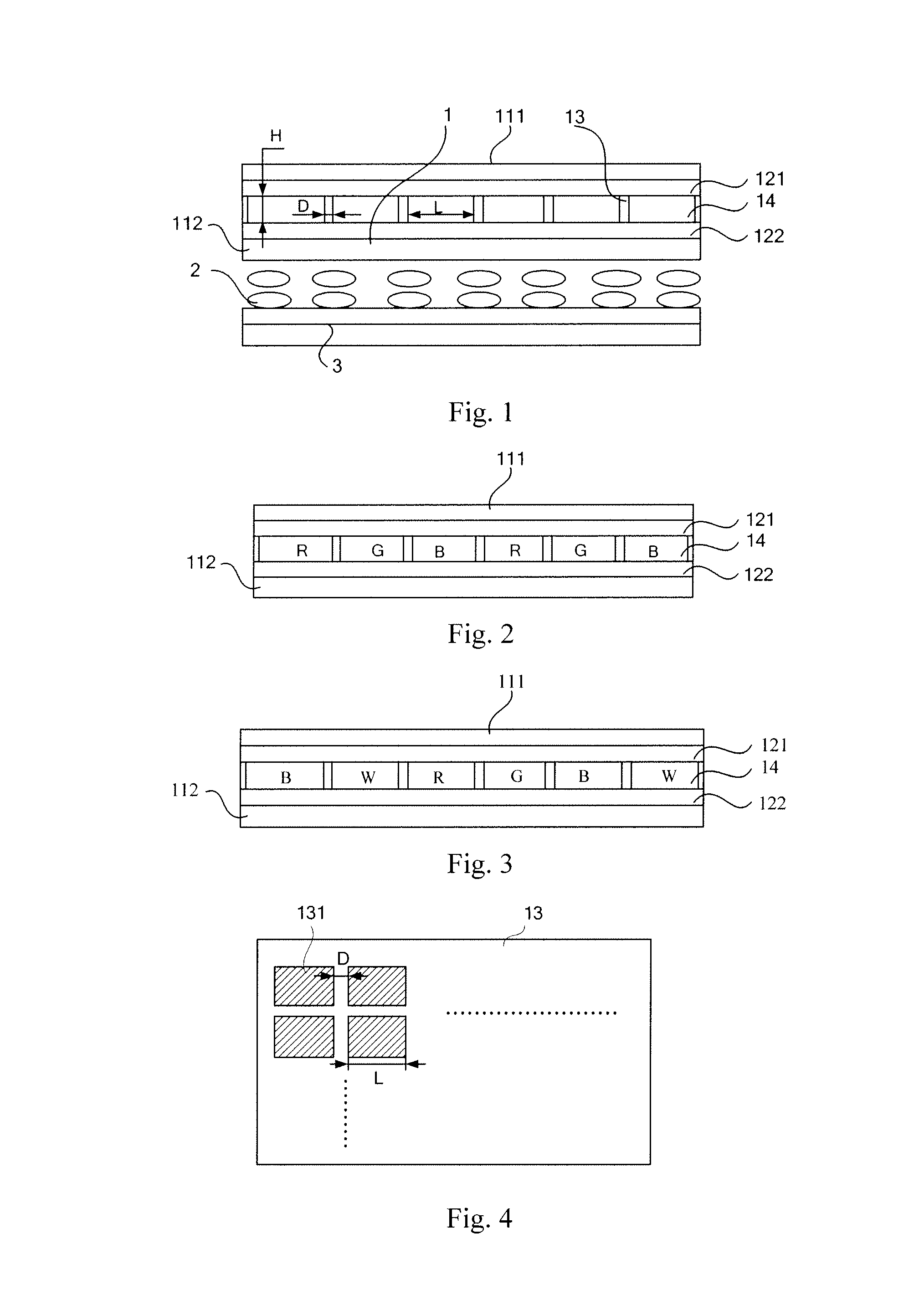
[0041]As shown in FIG. 1, the first embodiment of the present invention provides a color filter substrate 1, comprising: a first glass substrate 111, a first transparent electrode layer 121, a color filter 14, a black matrix 13, a second transparent electrode layer 122 and a second glass substrate 112, wherein the color filter 14 is made of electrochromic materials.
[0042]The color filter 14 comprises a plurality of pixel regions, and all these pixel regions are made of electrochromic materials. For example, the color filter 14 may comprise a red pixel region, a green pixel region and a blue pixel region. The red pixel region is made of electrochromic materials which are capable of changing to red, the green pixel region is made of electrochromic materials which are capable of changing to green, and the blue pixel region is made of electrochromic materials which are capable of changing to blue.
[0043]The color filter 14 may further comprise a white pixel region, which is formed of tra...
embodiment 2
[0057]On the basis of the above Embodiment 1 and its implementing manner, Embodiment 2 provides a LCD panel, as shown in FIG. 1. The LCD panel comprises an array substrate 3 and a color filter substrate 1 which are cell-assembled, and a liquid crystal molecular layer 2 between the array substrate 3 and the color filter substrate 1, and the second glass substrate 112 of the color filter substrate 1 disposed closer to the liquid crystal molecular layer 2 than the first glass substrate 111 of the color filter substrate 1. When the first and second transparent electrode layers 121, 122 are not powered on, each pixel region in the color filter 14 is transparent, and the color filter 14 has the maximum transmittance; and after the first and second transparent electrode layers 121, 122 are powered on, each of the pixel regions in the color filter 14 is changes from being transparent to a corresponding color which gradually deepens along with increasing the magnitude of the electric field b...
embodiment 3
[0059]The embodiment 3 provides a method of fabricating the color filter substrate 1, comprising the steps of:
[0060]Step S301: sputtering a first transparent electrode layer 121 on a first glass substrate 111;
[0061]Step S302: sputtering a second transparent electrode layer 122 on a second glass substrate 112;
[0062]Step S303: depositing a black matrix 13 on the second transparent electrode layer 122, and patterning the black matrix by etching;
[0063]Step S304: forming a color filter 14 by depositing or applying electrochromic materials in opening regions of the black matrix;
[0064]Step S305: cell-assembling the first and second glass substrates 111, 112, wherein the first transparent electrode layer 121 and the second glass substrate 122 are disposed opposite to each other.
[0065]In the color filter substrate 1 made by the method provided by the embodiment of the present invention, when the first and second transparent electrode layers 121, 122 are not powered on, each of the pixel regi...
PUM
| Property | Measurement | Unit |
|---|---|---|
| transmittance | aaaaa | aaaaa |
| thickness | aaaaa | aaaaa |
| thickness | aaaaa | aaaaa |
Abstract
Description
Claims
Application Information

