Organic light emitting diode display and manufacturing method thereof

a light-emitting diode and light-emitting diode technology, applied in the direction of thermoelectric device junction materials, semiconductor devices, electrical apparatus, etc., can solve the problems of low light extraction efficiency, achieve improved light efficiency, reduce color difference, and improve visibility

Active Publication Date: 2014-04-10
SAMSUNG DISPLAY CO LTD
View PDF1 Cites 2 Cited by
  • Summary
  • Abstract
  • Description
  • Claims
  • Application Information

AI Technical Summary

Benefits of technology

[0006]Aspects of embodiments of the present invention are directed to providing an organic light emitting diode display having increased light efficiency by differentiating structures for each pixel of red, green, and blue and improving visibility by reducing a color difference (WAD) according to an angle (e.g., a viewing angle) and a manufacturing method thereof.

Problems solved by technology

In addition, because a large part of the light emitted from the organic emission layer is guided in a direction parallel to a laminated surface due to total reflection (e.g., total internal reflection) and is lost, light extraction efficiency may be low.

Method used


Image

  • Organic light emitting diode display and manufacturing method thereof
  • Organic light emitting diode display and manufacturing method thereof
  • Organic light emitting diode display and manufacturing method thereof

Examples


Embodiment Construction

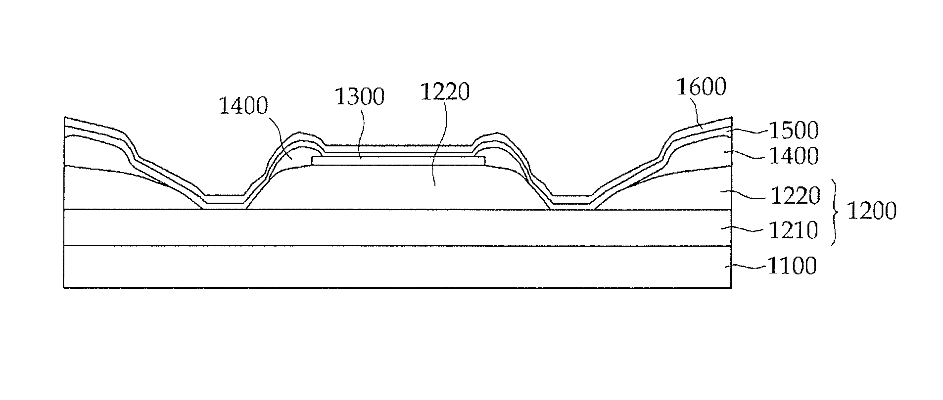
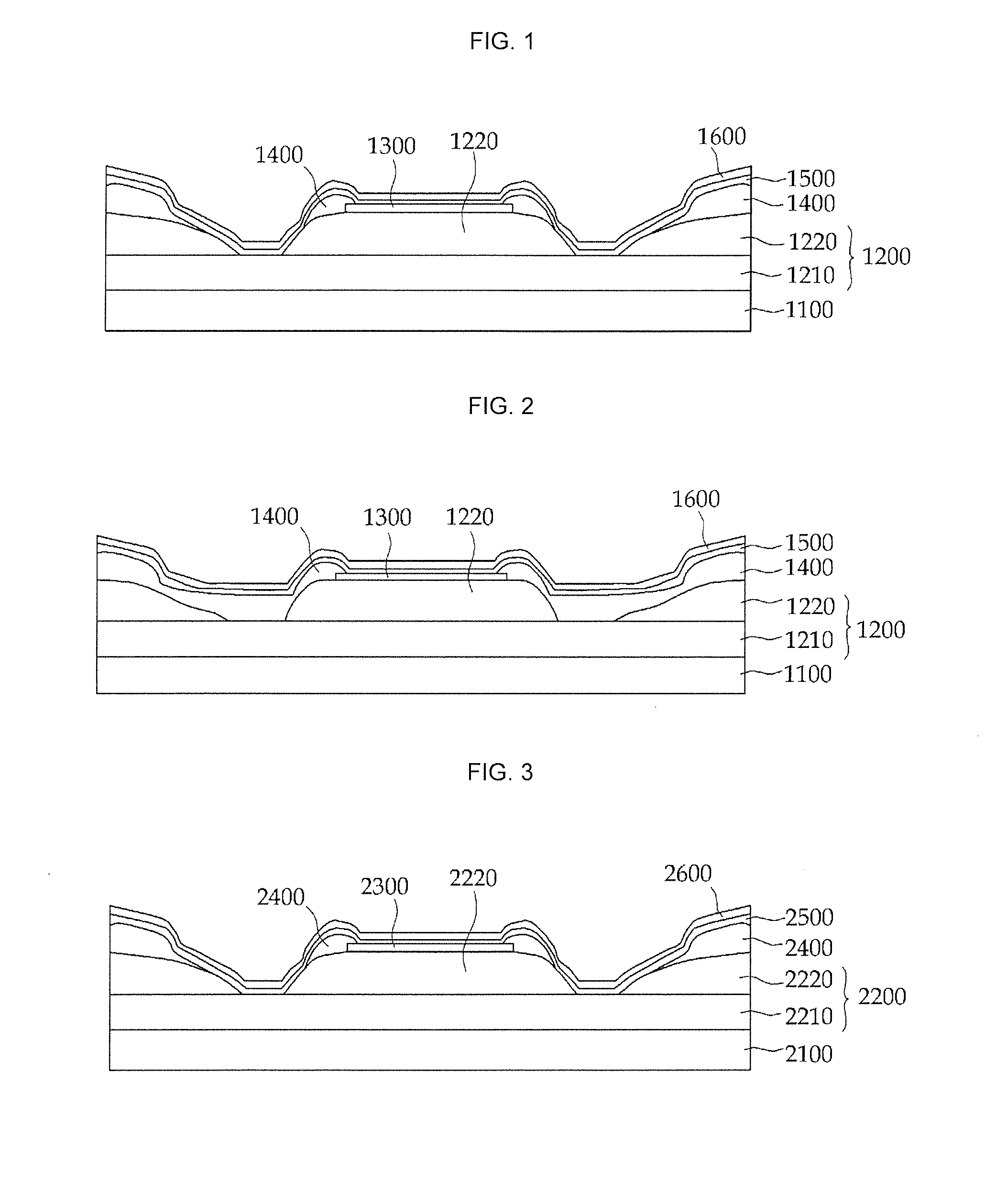
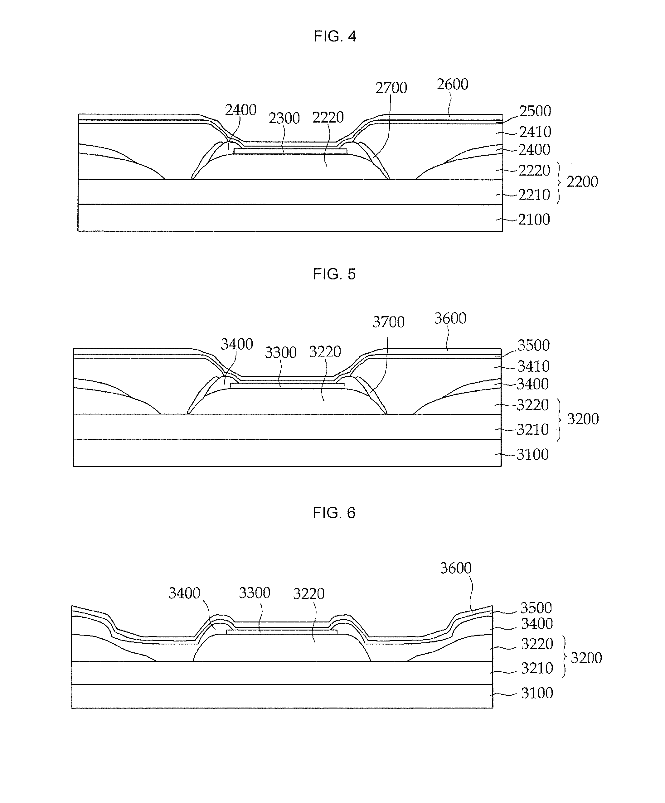
[0036]Hereinafter, exemplary embodiments of the present invention will be described in more detail with reference to the accompanying drawings.

[0037]Although embodiments of the present invention can be modified variously and have several embodiments, specific exemplary embodiments are illustrated in the accompanying drawings and will be mainly described in the specification. However, the scope of the present invention is not limited to the specific embodiments and should be construed as including all the changes, equivalents, and substitutions included in the spirit and scope of the present invention.

[0038]In this specification, specific structural or functional descriptions are provided to describe exemplary embodiments, and the exemplary embodiments of the present invention can be implemented in various forms. Embodiments of the present invention are not limited to the exemplary embodiments. It should be understood that the present invention contains all changes, equivalents, and ...


PUM


Abstract

An organic light emitting diode display includes: a substrate, an insulating layer on the substrate; a plurality of pixel electrodes on the insulating layer; a pixel defining layer on the insulating layer overlapping with an end of at least one of the pixel electrodes and defining an emission region and a non-emission region; an organic emission layer on the pixel electrodes; and a common electrode on the organic emission layer, wherein the insulating layer has a plurality of concave portions in the non-emission region adjacent corresponding ones of the pixel electrodes, wherein each of the concave portions has a bottom portion and an inclined portion, and wherein a reflective surface is on at least one of the inclined portions.

Description

CROSS-REFERENCE TO RELATED APPLICATIONS[0001]This application is based on and claims priority from Korean Patent Application No. 10-2012-0110557, filed on Oct. 5, 2012 in the Korean Intellectual Property Office, the entire disclosure of which is incorporated herein by reference.FIELD[0002]Embodiments of the present invention relate to an organic light emitting diode display and a manufacturing method thereof, and more particularly, to an organic light emitting diode display with enhanced light efficiency and visibility by differentiating structures for each pixel of red R, green G, and blue B and a manufacturing method thereof.BACKGROUND[0003]An organic light emitting diode display is a self-emission display device which has one or more organic light emitting diodes that emit light to display an image. Because the organic light emitting diode display does not require a separate light source unlike a liquid crystal display, it is possible to reduce a thickness and a weight of the dis...

Claims


Application Information

Patent Timeline
Patent Type & Authority Applications(United States)
IPC IPC(8): H01L51/52
CPCH01L51/52H10K59/35H10K59/122H10K59/124H10K50/856H10K50/80
Inventor CHOI, HAE-YUNLIM, JAE-IKKIM, MIN-WOOPARK, WON-SANG
Owner SAMSUNG DISPLAY CO LTD
Why Eureka
Try Eureka