Integrated diode array and corresponding manufacturing method

Active Publication Date: 2014-04-10
ROBERT BOSCH GMBH
View PDF22 Cites 0 Cited by
  • Summary
  • Abstract
  • Description
  • Claims
  • Application Information

AI Technical Summary

Benefits of technology

This patent text describes a new design for integrated diode arrays used in sensors. By using STI trenches, the diodes can be placed very close to each other, resulting in a smaller size of the sensor. This allows for more blocks or pixels to be placed on the same surface, increasing sensitivity. The diodes can also be made thinner, which reduces the time it takes to respond to light. Additionally, the gap between diodes can be minimized, further improving the performance of the sensor.

Problems solved by technology

However, this is at the expense of the space occupied by the sensor device and therefore has a restrictive effect on further integration.
However, this type of array is even more detrimental with regard to saving space.
However, such n-type doping regions require space and increase the complexity of the manufacturing method.

Method used


Image

  • Integrated diode array and corresponding manufacturing method
  • Integrated diode array and corresponding manufacturing method
  • Integrated diode array and corresponding manufacturing method

Examples


Embodiment Construction

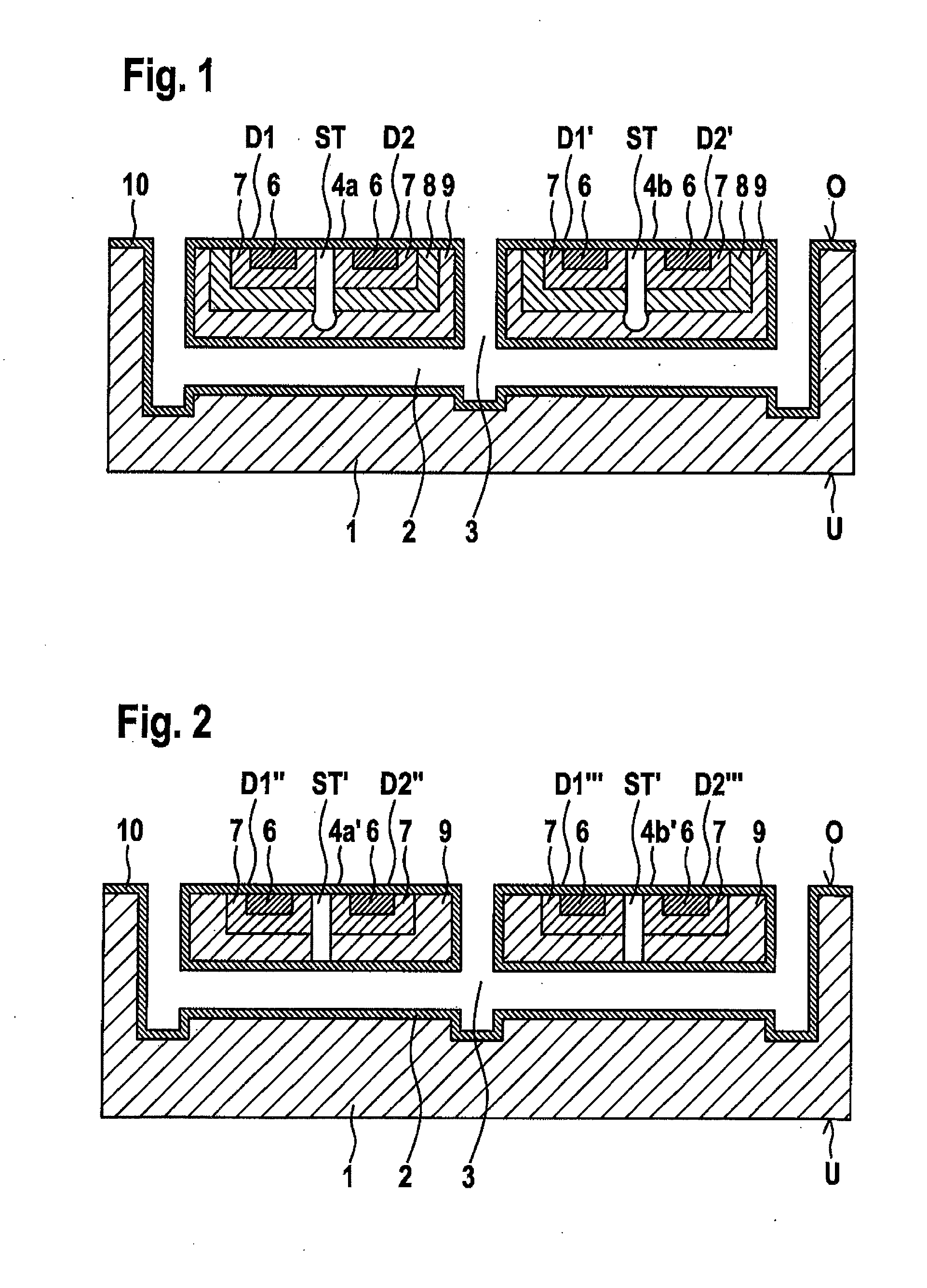
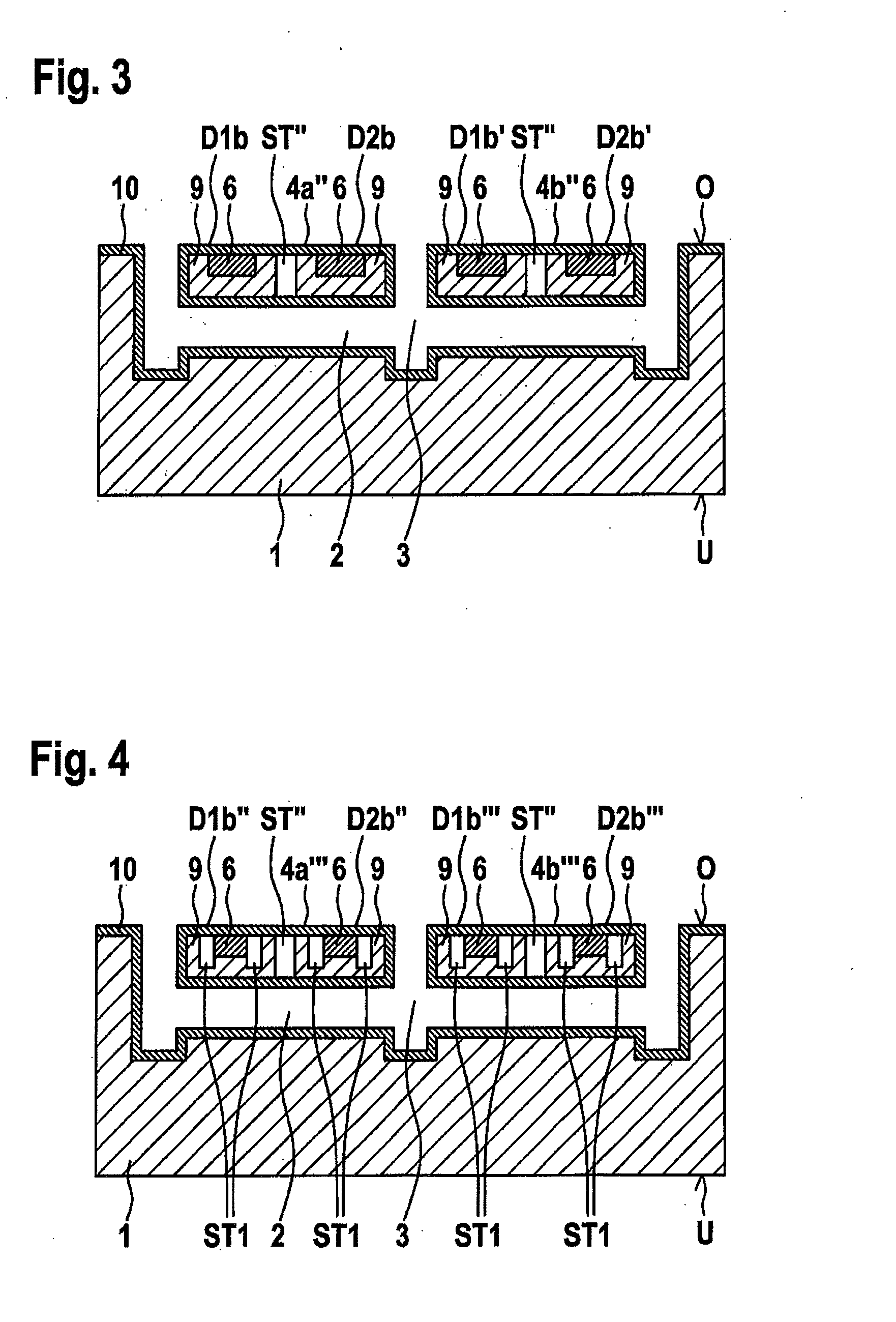
[0038]In the figures, identical or functionally equivalent elements are denoted by the same reference symbols.

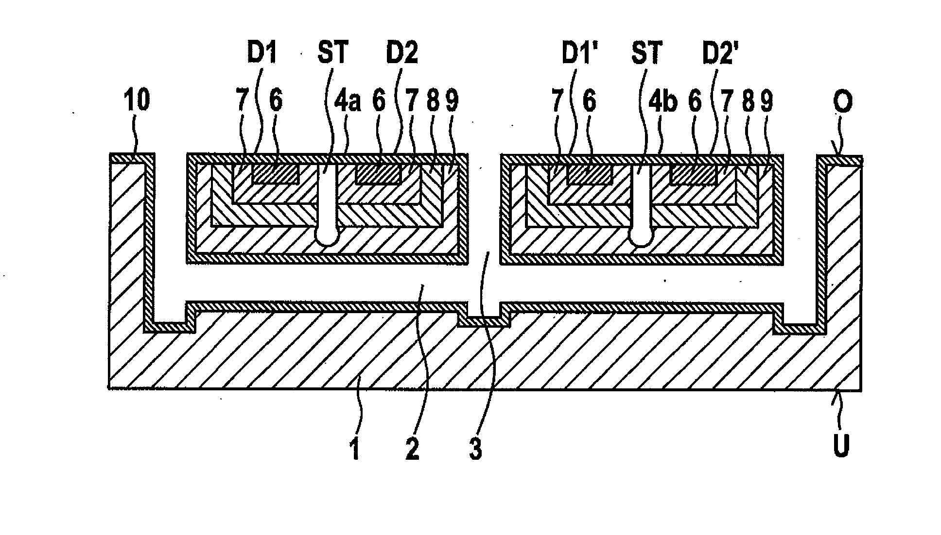
[0039]FIG. 1 shows a schematic vertical cross-sectional view of an integrated diode array according to a first exemplary embodiment of the present invention.

[0040]In FIG. 1, reference numeral 1 denotes a semiconductor substrate having an upper side O and a lower side U. A plurality of blocks 4a, 4b, of which only two blocks are shown in the view of FIG. 1, are suspended or anchored at substrate 1, above a cavity 2 situated beneath them in substrate 1. Blocks 4a, 4b are anchored to substrate 1 by oxide ribs (not shown).

[0041]Blocks 4a, 4b have a plurality of diodes D1, D2 and D1′, D2′, respectively, which are positioned in a planar manner and are, in the present exemplary embodiment, infrared diodes, the blocks 4a, 4b representing pixels of an infrared sensor device. Blocks 4a, 4b are separated from one another by respective gaps 3. In this context, the connection leads of th...


PUM


Abstract

An integrated diode array and a corresponding manufacturing method are provided. The integrated diode array includes a substrate having an upper side, and a plurality of blocks of several diodes, which are positioned in a planar manner and are suspended at the substrate above a cavity situated below them in the substrate. The blocks are separated from one another by respective gaps, and within a specific block, the individual diodes are electrically insulated from one another by first STI trenches situated between them.

Description

CROSS REFERENCE TO RELATED APPLICATION[0001]The present application claims priority to Application No. DE 10 2012 218 414.7, filed in the Federal Republic of Germany on Oct. 10, 2012, which is expressly incorporated herein in its entirety by reference thereto.FIELD OF INVENTION[0002]The present invention relates to an integrated diode array and a corresponding manufacturing method.BACKGROUND INFORMATION[0003]German Application No. DE 10 2008 054 481 describes an integrated diode array in the form of a sensor, which includes at least one micropatterned diode pixel that has a diode formed in, on or under a diaphragm, the diaphragm being formed above a cavity. The diode is contacted via leads, which are formed at least partially in, on or under the diaphragm, the diode being formed in a polycrystalline semiconductor layer.[0004]International Patent Publication No. WO 2007 / 147663 describes an infrared sensor having an array of diode pixels, each diode pixel having a monocrystalline regi...

Claims


Application Information

Patent Timeline
IPC IPC(8): H01L27/08H01L29/66
CPCH01L29/66136H01L27/0814G01J5/0225G01J5/024G01J5/0853H01L21/76229H01L21/76289H01L27/14649H01L2924/0002H01L2924/00G01J5/00H01L21/00H01L25/00H01L27/14
Inventor SCHUERMANN, GREGORBENZEL, HUBERT
Owner ROBERT BOSCH GMBH
Why Eureka
Try Eureka