
Printed circuit board, semiconductor package using the same, and method for manufacturing the printed circuit board and the semiconductor package

Inactive Publication Date: 2014-04-10
SAMSUNG ELECTRO MECHANICS CO LTD
View PDF3 Cites 2 Cited by
  • Summary
  • Abstract
  • Description
  • Claims
  • Application Information

AI Technical Summary

Benefits of technology

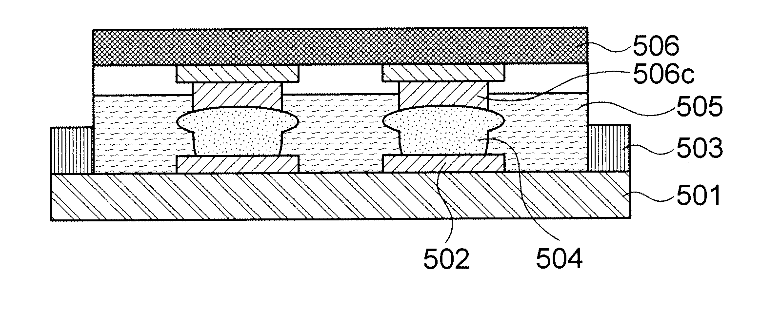
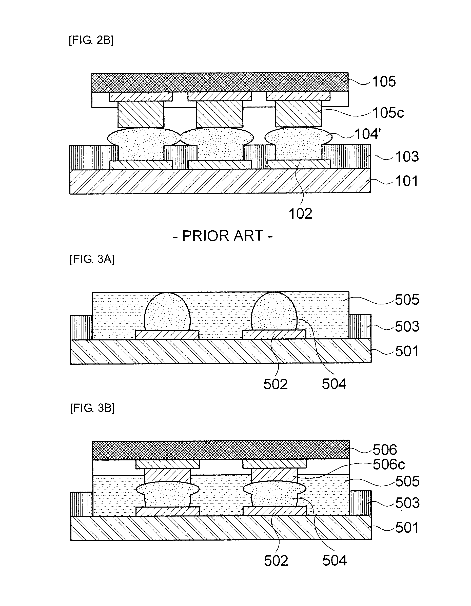
The present invention aims to solve problems in printed circuit board manufacturing, such as voids and short circuits between bumps. To achieve this, the invention provides a printed circuit board with a second insulating material that molds the PCB substrate before a semiconductor chip is bonded to it. A first insulating material is then formed to enclose the second insulating material and prevent it from leaking out. This method prevents the formation of voids and short circuits and improves the reliability of the printed circuit board.

Problems solved by technology

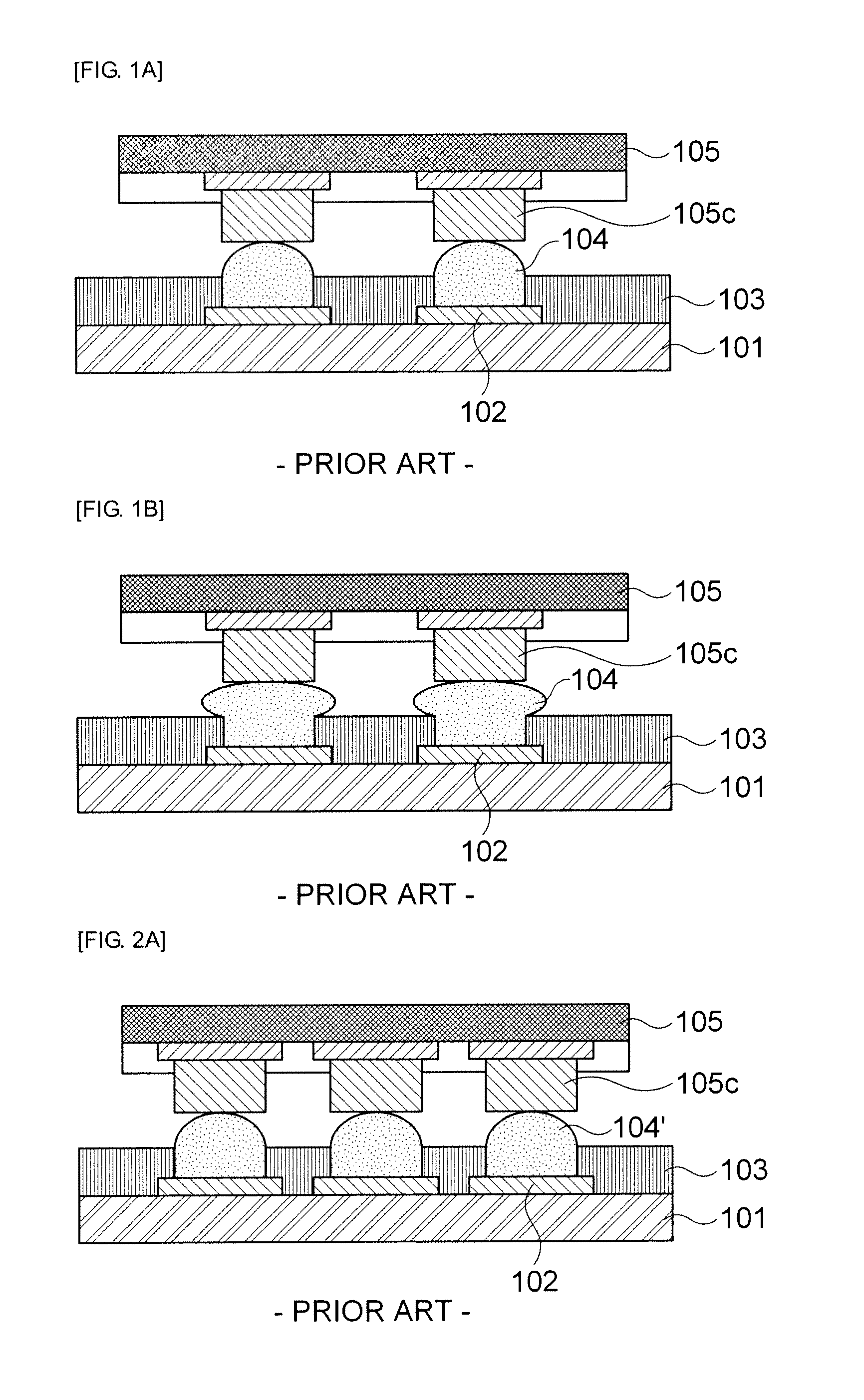
When applying the flip-chip bonding method, a bonding portion should be filled for high reliability, but as a bump pitch is continuously reduced, a void occurs when applying underfill, thus causing serious defects.
However, in a PCB manufacturing process, many side effects are derived due to the ink or film type solder resist used for this purpose.
Due to this, a solder resist residue exists in an undesired portion (selective open region), thus causing defects such as discoloration and non-plating.

Method used


Image

  • Printed circuit board, semiconductor package using the same, and method for manufacturing the printed circuit board and the semiconductor package
  • Printed circuit board, semiconductor package using the same, and method for manufacturing the printed circuit board and the semiconductor package
  • Printed circuit board, semiconductor package using the same, and method for manufacturing the printed circuit board and the semiconductor package

Examples


Embodiment Construction

[0049]The terms or words used in the present specification and claims should not be interpreted as being limited to typical or dictionary meanings, but should be interpreted as having meanings and concepts relevant to the technical spirit of the present invention based on the rule according to which an inventor can appropriately define the concept of the term to describe his / her own invention in the best manner.

[0050]Throughout the specification, when an element is referred to as “including” another element, it can further include the other element rather than exclude the other element unless the context clearly indicates otherwise. Further, the terms “unit”, “module”, “apparatus”, etc. used in the present specification represent a unit for processing at least one function or operation and may be implemented by hardware, software, or a combination thereof.

[0051]Hereinafter, embodiments of the present invention will be described in detail with reference to the accompanying drawings.

[...


PUM

PropertyMeasurementUnit
Electrical conductoraaaaaaaaaa
aaaaaaaaaa

Abstract

The present invention relates to a printed circuit board, a semiconductor package using the same, and a method for manufacturing the printed circuit board and the semiconductor package. The method for manufacturing a semiconductor package in accordance with the present invention includes: forming a circuit of a predetermined pattern on a PCB substrate; applying a first insulating material on the substrate; removing the first insulating material in the remaining portion except a predetermined portion by exposing and developing the substrate; forming a solder bump in the circuit portion exposed; molding a certain region of an upper surface portion of the PCB substrate including the solder bump by filling a second insulating material on the PCB substrate including the circuit portion; mounting a semiconductor chip on the PCB substrate; and completing one package in which the semiconductor chip and the PCB substrate are integrated.

Description

CROSS-REFERENCE TO RELATED APPLICATIONS[0001]Claim and incorporate by reference domestic priority application and foreign priority application as follows:Cross Reference To Related Application[0002]This application claims the benefit under 35 U.S.C. Section 119 of Korean Patent Application Serial No. 10-2012-0110678, entitled filed Oct. 5, 2012, which is hereby incorporated by reference in its entirety into this application.BACKGROUND OF THE INVENTION[0003]1. Field of the Invention[0004]The present invention relates to a printed circuit board, a semiconductor package using the same, and a method for manufacturing the printed circuit board and the semiconductor package, and more particularly, to a printed circuit board, a semiconductor package using the same, and a method for manufacturing the printed circuit board and the semiconductor package that can overcome occurrence of a void due to an underfill process after flip-chip interconnection and occurrence of a short between bumps wh...

Claims


Application Information

Patent Timeline
IPC IPC(8): H01L23/00H05K3/10H05K1/18H05K1/03H05K3/40
CPCH01L24/17H01L24/81H05K3/10H05K3/4007H05K1/181H05K1/0313H05K3/3436H05K3/3452H05K2201/10977H01L21/563H01L24/13H01L24/16H01L24/29H01L24/32H01L24/83H01L24/91H01L2224/26175H01L2224/2919H01L2224/73204H01L2224/81193H01L2224/81203H01L2224/83192H01L2224/83203H01L2224/83856H01L2224/83862H01L2224/131H01L2224/32225H01L2224/8385H01L2224/9211H01L2224/81903Y10T29/49158Y02P70/50H01L2924/0665H01L2924/00014H01L2924/014H01L2224/81H01L2224/83H01L23/12
Inventor KIM, YOUNG SOONKIM, JUN HAN
Owner SAMSUNG ELECTRO MECHANICS CO LTD
Learn More