Electronic module with heat spreading enclosure

Active Publication Date: 2014-04-17
MICROELECTRONICS ASSEMBLY TECH
View PDF18 Cites 14 Cited by
  • Summary
  • Abstract
  • Description
  • Claims
  • Application Information

AI Technical Summary

Benefits of technology

[0018]In accordance with another aspect of the invention, an electronic subsystem comprises: a rigid circuit board daughter card or substrate having a plurality of electrical components on at least one surface thereof and electrical contacts along one edge thereof, one or more flexible circuit leads having a plurality of electrical contacts in electrical communication with the electrical contacts of the rigi

Problems solved by technology

As the number of lines increases, and the pitch becomes corresponding

Method used


Image

  • Electronic module with heat spreading enclosure
  • Electronic module with heat spreading enclosure
  • Electronic module with heat spreading enclosure

Examples


example

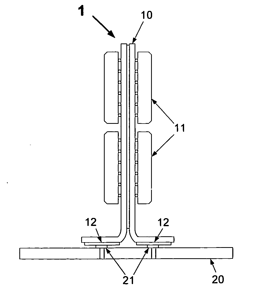
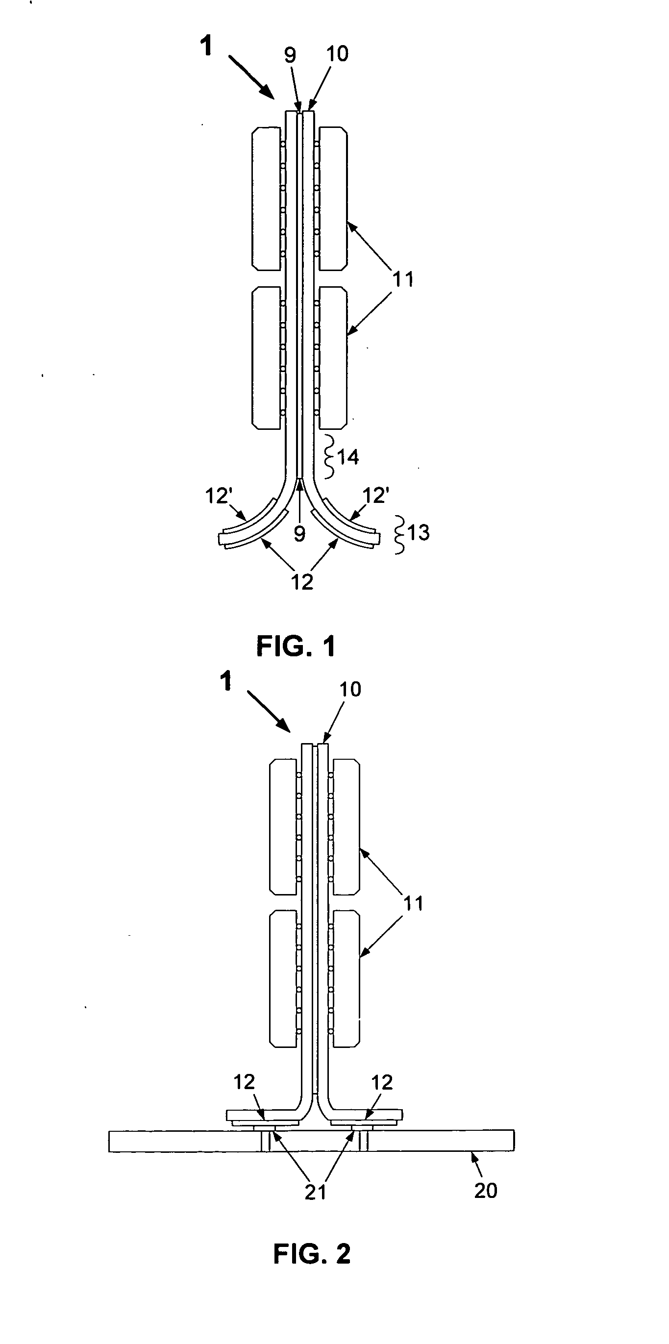
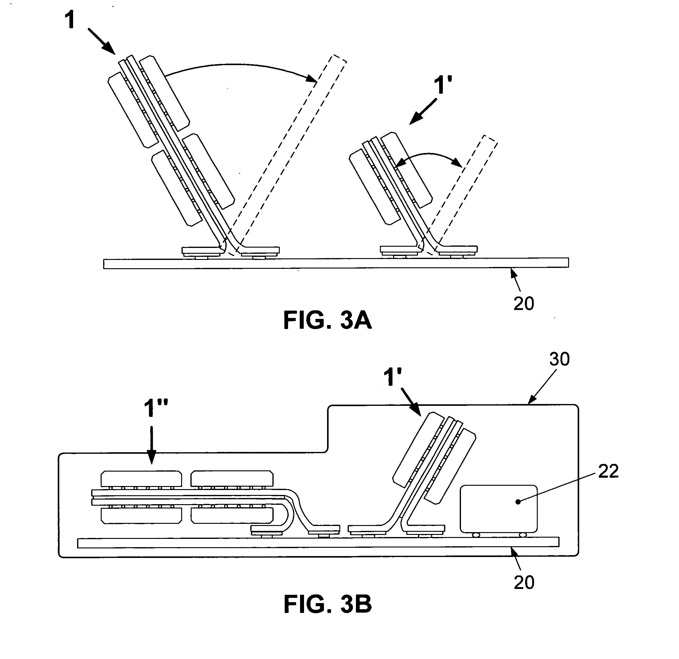
[0084]The inventive circuit is preferably manufactured as follows. First, two individual flexible circuit plies or laminates having conductive traces (typically on both surfaces) and vias connecting one surface to the other and one ply to another as needed, are formed by conventional means and bonded together over most of their surface area to form a multilayer flex panel or circuit board, leaving an unbonded strip (bifurcation) along one edge. The electrode pads intended to connect this circuit to a motherboard are located on the inner surfaces of the bifurcation. Next, the flex circuit is populated by microelectronic devices, which may be any combination of analog, digital, or mixed-mode semiconductor devices or passive components. This step will typically involve conventional “pick and place” assembly using solder or conductive adhesives as are known in the art. Then, the two legs of the bifurcated extensions or area are spread apart and the electrode pads are aligned with rows o...


PUM

PropertyMeasurementUnit
Angleaaaaaaaaaa
Angleaaaaaaaaaa
Flexibilityaaaaaaaaaa

Abstract

An electronic module comprises: a multilayer circuit board having a bifurcated area along one edge and a plurality of electronic components mounted on at least one surface; a plurality of electrode pads functionally connected to the electronic components and positioned on the inner surfaces of the bifurcated area so that when the two legs of the bifurcated area are spread apart by about 180° the electrode pads align with respective contacts on a motherboard, and are connectable thereto, so that a secure connection may be created between the circuit board and the motherboard; and, two metal, heat spreading covers lockably enclosing the circuit board, one on either side, the covers further providing mating surfaces upon which a mechanical clamping device can engage and secure the module to a motherboard.

Description

CROSS REFERENCE TO RELATED APPLICATIONS[0001]This application is related to the following U.S. patent applications, filed on even date herewith by the present inventors: Docket No. MAT-20A, entitled “Flexible circuit board and connection system”; Docket No. MAT-20B, entitled “Rigid circuit board with flexibly attached module”; Docket No. MAT-20C, entitled “Method for making an electrical circuit”; Docket No. MAT-20E entitled “Electronic interconnect system”; Docket No. MAT-20F entitled “Pierced flexible circuit and compression joint”; and Docket No. MAT-20G entitled “Compression connector system.” The entire disclosures of each of the foregoing are incorporated herein by reference.BACKGROUND OF THE INVENTION[0002]1. Field of the Invention[0003]The present invention relates generally to means for connecting microelectronic devices and systems. More particularly, the invention relates to improved flex-circuit based interconnect solutions for electronic circuits.[0004]2. Description of...

Claims


Application Information

Patent Timeline
IPC IPC(8): H05K7/20H05K3/10G06F1/20
CPCG06F1/20H01R12/62H01R12/737H05K1/118H05K1/147H05K3/366H05K2201/046H05K2201/09481H05K2201/10159H05K2201/10189H05K2201/10409H05K2201/10545Y10T29/49149Y10T29/49155Y10T29/49147Y10T29/49126
Inventor CLAYTON, JAMES E.FATHI, ZAKARYAE
Owner MICROELECTRONICS ASSEMBLY TECH
Why Eureka
Try Eureka