
Stacked chip module with integrated circuit chips having integratable and reconfigurable built-in self-maintenance blocks

a technology of integrated circuit chips and modules, applied in the direction of basic electric elements, semiconductor/solid-state device testing/measurement, instruments, etc., can solve the problem of occupying a significant amount of surface area

Active Publication Date: 2014-04-24
IBM CORP
View PDF0 Cites 7 Cited by
  • Summary
  • Abstract
  • Description
  • Claims
  • Application Information

AI Technical Summary

Benefits of technology

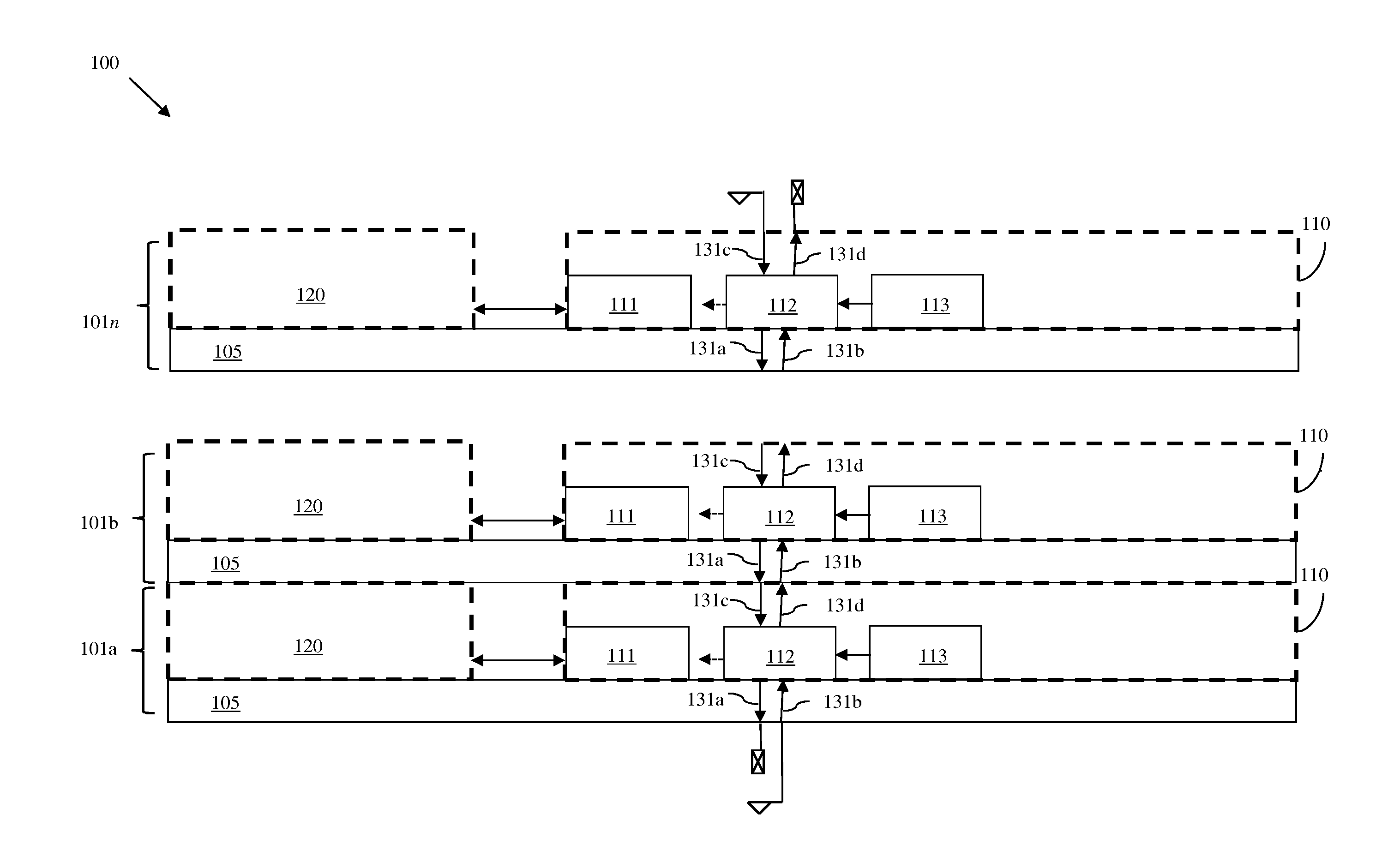
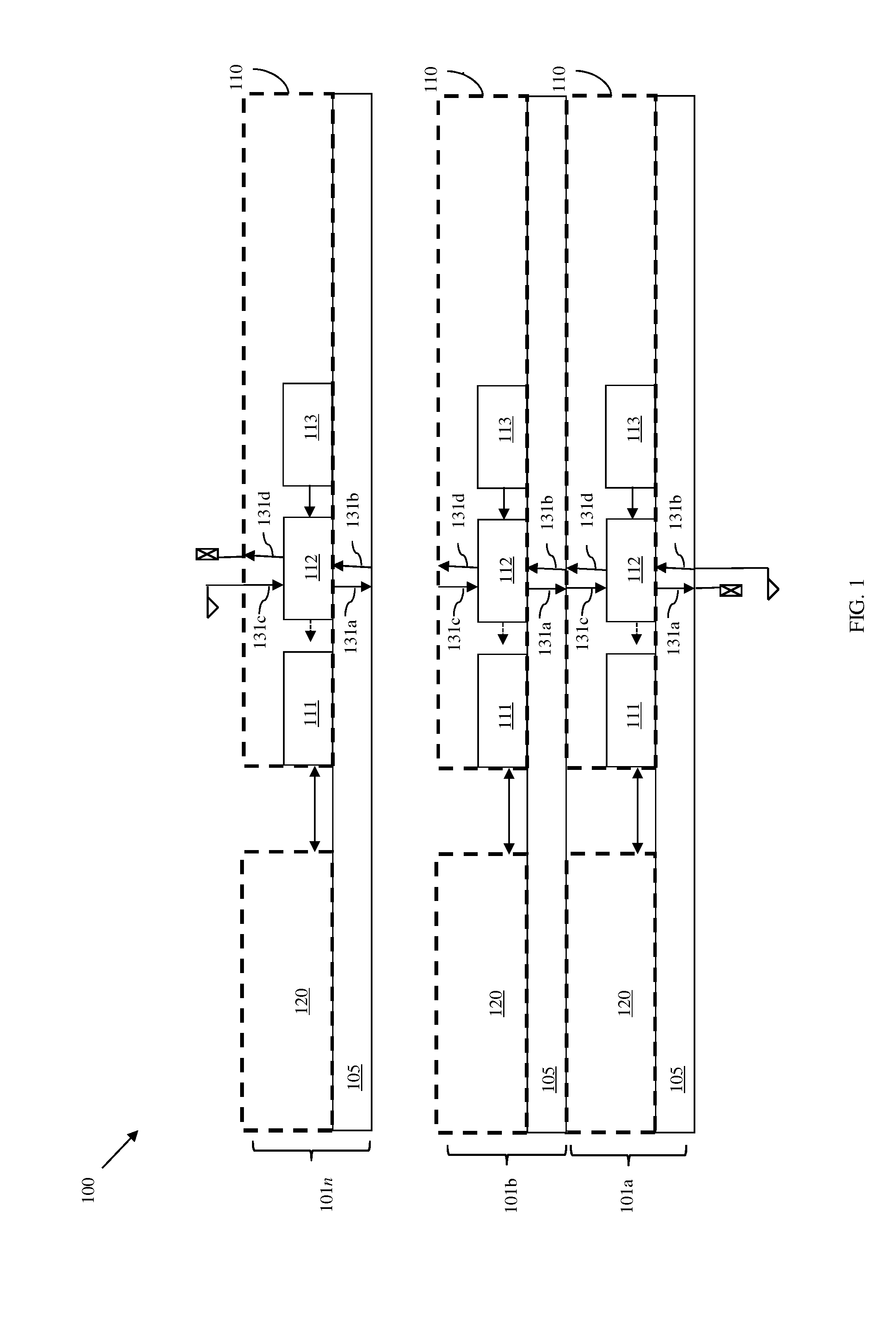
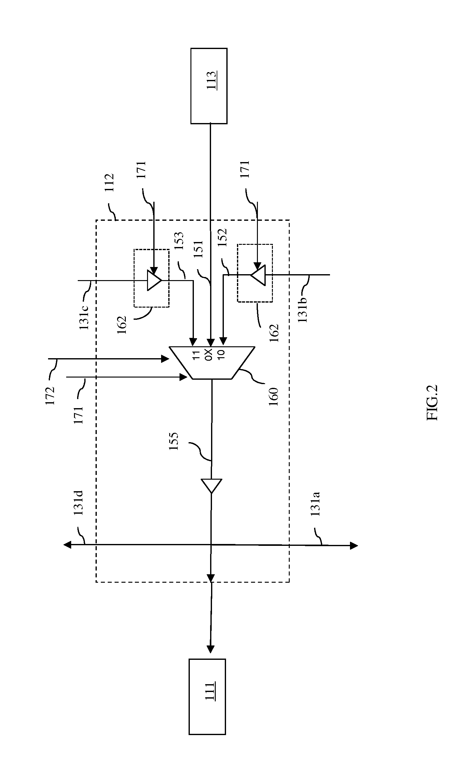
The patent describes a stacked chip module that incorporates built-in self-maintenance blocks with reconfiguration circuitry for servicing functional blocks at the module level. The self-maintenance blocks allow for automatic servicing of functional blocks during wafer-level and module-level servicing. The reconfiguration circuitry can automatically and selectively enable either the built-in self-maintenance circuitry or another controller on the same or another chip in the stack to control servicing of the functional block. The method also includes manufacturing and servicing the stacked chip module. The technical effect of this invention is to provide efficient and flexible servicing of integrated circuit chips in a stacked chip module.

Problems solved by technology

When individual integrated circuit (IC) chips are mounted side-by-side on a printed circuit board (PCB), they take up a significant amount of surface area.
Unfortunately, self-maintenance (i.e., self-servicing, such as self-testing and / or self-repairing) of the individual IC chips on a stacked chip module presents a number of special challenges and such self-maintenance is can be critical to ensure product reliability.

Method used


Image

  • Stacked chip module with integrated circuit chips having integratable and reconfigurable built-in self-maintenance blocks
  • Stacked chip module with integrated circuit chips having integratable and reconfigurable built-in self-maintenance blocks
  • Stacked chip module with integrated circuit chips having integratable and reconfigurable built-in self-maintenance blocks

Examples


Embodiment Construction

[0027]As mentioned above, individual integrated circuit (IC) chips are mounted side-by-side on a printed circuit board (PCB), they take up a significant amount of surface area. Additionally, signals are typically passed from IC chip to IC chip on the PCB through large high-power, high-speed links. Recently developed stacked chip modules (also referred to herein as stacked chip packages, three-dimensional (3D) chip stacks or 3D multi-chip modules) allow for reductions in form factor, interface latency and power consumption as well as an increase in bandwidth. These benefits stem from the fact that, within a stacked chip module, signals are passed through the IC chips using simple wire-based interconnects (e.g., through substrate vias (TSVs) and micro-controlled collapsed chip connections (C4-connections)). Thus, there is a reduction in wire delay, which results in corresponding reductions in interface latency and power consumption as well as an increase in bandwidth. Unfortunately, s...


PUM


Abstract

Disclosed is a stacked chip module incorporating a stack of integrated circuit (IC) chips having integratable and automatically reconfigurable built-in self-maintenance blocks (i.e., built-in self-test (BIST) circuits or built-in self-repair (BISR) circuits). Integration of the built-in self-maintenance blocks between the IC chips in the stack allows for servicing (e.g., self-testing or self-repairing) of functional blocks at the module-level. Automatic reconfiguration of the built-in self-maintenance blocks further allows for functional blocks on any of the IC chips in the stack to be serviced at the module-level even when one or more controllers associated with a given built-in self-maintenance block on a given IC chip has been determined to be defective (e.g., during previous wafer-level servicing). Also disclosed is a method of manufacturing and servicing such a stacked chip module.

Description

BACKGROUND[0001]1. Field of the Invention[0002]The disclosed embodiments relate to stacked chip modules and, more particularly, to a stacked chip module with integrated circuit (IC) chips having integratable and reconfigurable built-in self-maintenance blocks (i.e., built-in self-test (BIST) blocks or built-in self-repair (BISR) blocks).[0003]2. Description of the Related Art[0004]When individual integrated circuit (IC) chips are mounted side-by-side on a printed circuit board (PCB), they take up a significant amount of surface area. Additionally, signals are typically passed from IC chip to IC chip on the PCB through large high-power, high-speed links. Recently developed stacked chip modules (also referred to herein as stacked chip packages, three-dimensional (3D) chip stacks or 3D multi-chip modules) allow for reductions in form factor, interface latency and power consumption as well as an increase in bandwidth. These benefits stem from the fact that, within a stacked chip module,...

Claims


Application Information

Patent Timeline
Patent Type & Authority Applications(United States)
IPC IPC(8): H01L23/52H01L21/66
CPCH01L23/525G11C5/04G11C29/006G11C29/4401G11C29/88G01R31/3187H01L2924/0002H01L25/0657H01L2924/00H01L22/34
Inventor GORMAN, KEVIN W.MONDAL, KRISHNENDUSETHURAMAN, SARAVANAN
Owner IBM CORP
Learn More