Pattern forming method, multi-layered resist pattern, multi-layered film for organic solvent development, resist composition, method for manufacturing electronic device, and electronic device

a technology of resist composition and pattern, applied in the field of pattern forming method, can solve the problem of pattern being liable to have an undercut profil

Active Publication Date: 2014-04-24
FUJIFILM CORP
View PDF3 Cites 18 Cited by
  • Summary
  • Abstract
  • Description
  • Claims
  • Application Information

AI Technical Summary

Benefits of technology

[0008]The present inventors have found that according to a negative pattern forming method by organic solvent development, for example, the pro

Problems solved by technology

However, the negative pattern forming method by organic solvent developme

Method used


Image

  • Pattern forming method, multi-layered resist pattern, multi-layered film for organic solvent development, resist composition, method for manufacturing electronic device, and electronic device
  • Pattern forming method, multi-layered resist pattern, multi-layered film for organic solvent development, resist composition, method for manufacturing electronic device, and electronic device
  • Pattern forming method, multi-layered resist pattern, multi-layered film for organic solvent development, resist composition, method for manufacturing electronic device, and electronic device

Examples


synthesis example 1

Synthesis of Resin (pol-1)

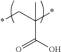
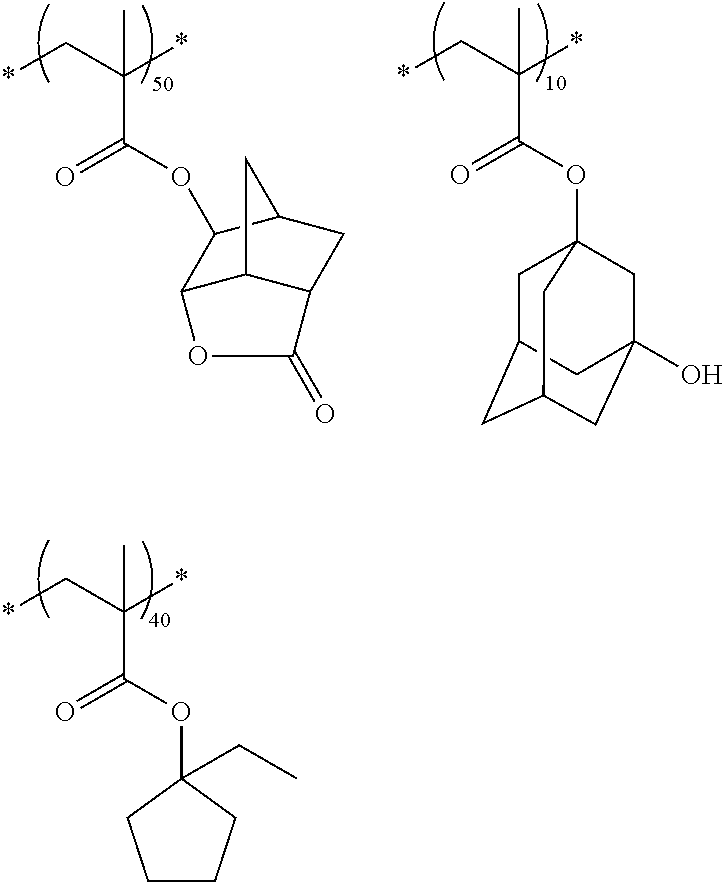
[0769]In a nitrogen stream, 61.2 parts by mass of cyclohexanone was charged into a three-neck flask and heated at 80° C. Subsequently, a mixed solution containing a monomer (15.0 parts by mass) corresponding to unit-1 shown below, a monomer (3.54 parts by mass) corresponding to unit-5 shown below, a monomer (12.3 parts by mass) corresponding to unit-22 shown below, and 1.38 parts by mass of dimethyl 2,2′-azobisisobutyrate [V-601, produced by Wako Pure Chemical Industries, Ltd.], and cyclohexanone (113.6 parts by mass) was added dropwise to the flask over 4 hours. After the completion of dropwise addition, the reaction was further allowed to proceed at 80° C. for 2 hours. The reaction solution was left standing to cool, reprecipitated in a large amount of heptane / ethyl acetate (8 / 2 by mass) and filtered, and the obtained solid was vacuum-dried to obtain 27.4 parts by mass of Resin (pol-1). The weight average molecular weight of Resin (pol-1) obtained was 12,...

example b

ArF Exposure Example B

Examples 45 to 52 and Comparative Example 4

[0784]An organic antireflection film, ARC29A (produced by Nissan Chemical Industries, Ltd.), was coated on a silicon wafer and baked at 205° C. for 60 seconds to form an antirefleetion film having a thickness of 86 nm, and the first resist composition shown in Table 12 below was coated thereon and baked (Pre-Bake: PB) under the conditions shown in Table 12 below to form a first-layer (lower-layer) resist film having the thickness shown in Table 12 below. Subsequently, the second resist composition was coated on the obtained first-layer resist film and baked (Pre-Bake: PB) under the conditions shown in Table 12 below to form a second-layer (upper-layer) resist film having the thickness shown in Table 12 below. In this way, a wafer on which two resist film layers are stacked was obtained.

[0785]The obtained wafer was patternwise exposed through a halftone mask having a line-and-space pattern with a light-shielding part wi...


PUM


Abstract

There is provided a pattern forming method comprising: (i) a step of forming a first film on a substrate by using a first resin composition (I), (ii) a step of forming a second film on the first film by using a second resin composition (II) different from the resin composition (I), (iii) a step of exposing a multi-layered film having the first film and the second film, and (iv) a step of developing the first film and the second film in the exposed multi-layered film by using an organic solvent-containing developer to form a negative pattern.

Description

CROSS REFERENCE TO RELATED APPLICATION[0001]This is a continuation of International Application No. PCT / JP2012 / 067139 filed on Jun. 28, 2012, and claims priority from Japanese Patent Application No. 2011-146861 filed on Jun. 30, 2011, U.S. provisional application. No. 61 / 503,048 filed on Jun. 30, 2011, and Japanese patent application No. 2012-143050 filed on Jun. 26, 2012, the entire disclosures of which are incorporated therein by reference.TECHNICAL FIELD[0002]The present invention relates to a pattern forming method suitably used for the process of producing a semiconductor such as IC or the production of a liquid crystal device or a circuit board such as thermal head and further for the lithography in other photo-fabrication processes, a multi-layered resist pattern, a multi-layered film for organic solvent development, a resist composition suitably used for the pattern forming method, a manufacturing method of an electronic device, and an electronic device. In particular, the p...

Claims


Application Information

Patent Timeline
IPC IPC(8): G03F7/32
CPCG03F7/325G03F7/0392G03F7/0397G03F7/095H01L21/0274
Inventor KATO, KEITASHIRAKAWA, MICHIHIROODANI, TADAHIRONAKAMURA, ATSUSHITAKAHASHI, HIDENORIIWATO, KAORU
Owner FUJIFILM CORP
Why Eureka
Try Eureka