Compensating for warpage of a flip chip package by varying heights of a redistribution layer on an integrated circuit chip

a technology of integrated circuit chips and redistribution layers, which is applied in the direction of electrical equipment, semiconductor devices, semiconductor/solid-state device details, etc., can solve the problems of warpage of flip chip joints or cu pillars, the effect of affecting the warpage of flip chip joints

Inactive Publication Date: 2014-05-01
GLOBALFOUNDRIES INC
View PDF6 Cites 14 Cited by
  • Summary
  • Abstract
  • Description
  • Claims
  • Application Information

AI Technical Summary

Problems solved by technology

The combination of these requirements results in greater complexity of semiconductor packaging design.
During the first phase of packaging, the flip chip-join of the solder bumps or Cu pillars is adversely affected by warpage, which varies as a function of temperature.
At peak elevated temperatures, the solder bumps or Cu pillars above the edges and corners of the IC chip, and the solder of the opposing FC attaches are physically separated and contact is impossible.
Experiments indicate that warpage above the edges and corners of the IC chip results in gaps of 10 or more microns between the surfaces of the solder bumps or Cu pillars and their corresponding FC attaches in a flip chip package.
Such a gap results in a warpage-related “nonwet” problem, where the opposing miscible solders cannot mix.
The mechanical stresses and strains that occur with chip package interactions (CPIs) are complex, depending upon many factors including IC chip design, chip carrier design, process variations in IC chip and chip carrier manufacture, and process variations in bond and assembly.
Many CPIs result from stress / strain caused by a mismatch between the coefficients of thermal expansion (CTE) of the IC chip and the chip carrier during the processes of heating the solder of the solder bumps or CU pillars to their melting point and the subsequent cooling of the joined IC chip and chip carrier to an ambient temperature.
Differences in contraction during cool-down result in shear forces between the IC chip and the chip carrier.
White bumps typically occur at the IC chip's edges and corners, where shear forces resulting from warpage are greatest.
However, fabrication of an RDL structure with two full-thickness continuous polyimide layers, each of approximately 10 μm thickness, subsequently gives rise to unacceptable levels of IC chip-side warpage from polyimide tensile stresses during flip chip packaging.

Method used


Image

  • Compensating for warpage of a flip chip package by varying heights of a redistribution layer on an integrated circuit chip
  • Compensating for warpage of a flip chip package by varying heights of a redistribution layer on an integrated circuit chip
  • Compensating for warpage of a flip chip package by varying heights of a redistribution layer on an integrated circuit chip

Examples


Embodiment Construction

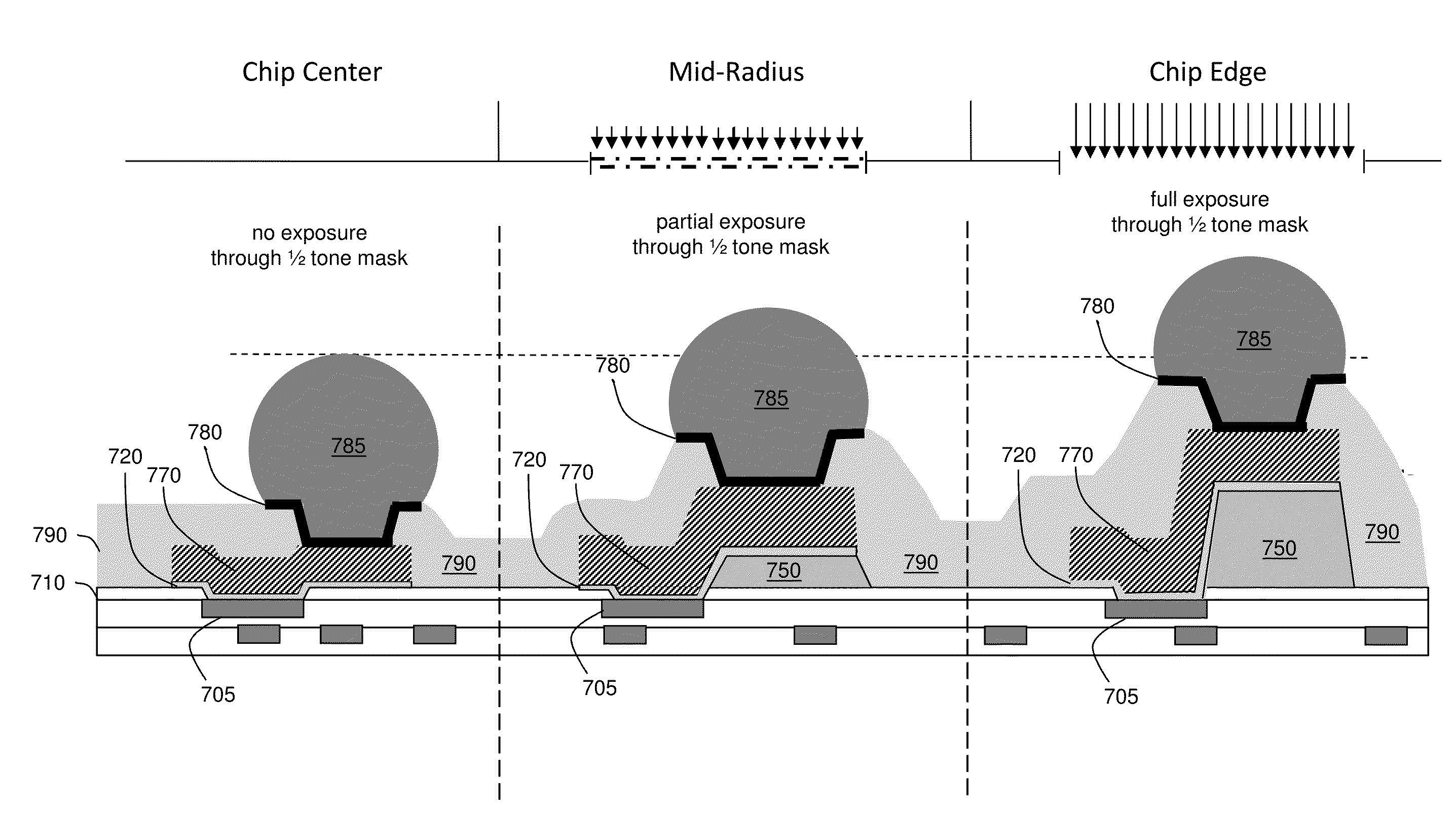
[0030]The exemplary embodiments of the disclosure and their various features and advantageous details are explained more fully with reference to the non-limiting exemplary embodiments that are illustrated in the accompanying drawings and detailed in the following description. It should be noted that the features illustrated in the drawings are not necessarily drawn to scale. Descriptions of well-known materials, components, and processing techniques are omitted so as to not unnecessarily obscure the exemplary embodiments of the disclosure. The examples used herein are intended to merely facilitate an understanding of ways in which the exemplary embodiments of the disclosure may be practiced and to further enable those of skill in the art to practice the exemplary embodiments of the disclosure. Accordingly, the examples should not be construed as limiting the scope of the exemplary embodiments of the disclosure.

[0031]As described above, there remains a need to compensate for the gap ...


PUM


Abstract

Structures and methods of making a flip chip package that employ polyimide pads of varying heights at a radial distance from a center of an integrated circuit (IC) chip for a flip chip package. The polyimide pads may be formed under electrical connectors, which connect the IC chip to a chip carrier of the flip chip package, so that electrical connectors formed on polyimide pads of greater height are disposed at a greater radial distance from the center of the IC chip, while electrical connectors formed on polyimide pads of a lesser height are disposed more proximately to the center of the IC chip. Electrical connectors of a greater relative height to the IC chip's surface may compensate for a gap, produced by heat-induced warpage during the making of the flip chip package, that separates the electrical connectors on the IC chip from flip chip attaches on the chip carrier.

Description

BACKGROUND[0001]1. Field of the Invention[0002]This disclosure generally relates to structures of a chip-side redistribution layer (RDL) and methods of making a chip-side RDL that employ polyimide pads of varying heights at a radial distance from a center of an integrated circuit (IC) chip for a flip chip package. The polyimide pads of varying heights may be formed under electrical connectors, which connect the IC chip to a chip carrier of the flip chip package, so that those electrical connectors formed on polyimide pads of a greater height are disposed at a greater radial distance from the center of the IC chip, i.e., on the IC chip's edges and corners, while electrical connectors formed on polyimide pads of a lesser height are disposed more proximately to the center of the IC chip. Electrical connectors of a greater relative height to the IC chip's surface may compensate for a gap, produced by warpage, that separates the electrical connectors on the IC chip from flip chip attache...

Claims


Application Information

Patent Timeline
Patent Type & Authority Applications(United States)
IPC IPC(8): H01L23/498H01L21/50
CPCH01L23/525H01L24/13H01L24/14H01L2224/16225H01L2924/15174H01L2924/15311H01L23/562H01L2224/05569H01L2224/024H01L2224/0236H01L23/3192H01L24/05H01L24/06H01L24/16H01L2224/02331H01L2224/02381H01L2224/0239H01L2224/0401H01L2224/05573H01L2224/05575H01L2224/05618H01L2224/05639H01L2224/05644H01L2224/05655H01L2224/05671H01L2224/06102H01L2224/13147H01L2924/3511H01L2224/05572H01L2924/00014H01L2924/12042H01L23/3114H01L2224/02125H01L2224/05552H01L2924/00H01L24/11H01L2224/0231H01L2224/11848H01L2924/07025H01L2924/14H01L2924/1531
Inventor DAUBENSPECK, TIMOTHY H.GAMBINO, JEFFREY P.MUZZY, CHRISTOPHER D.SAUTER, WOLFGANGSULLIVAN, TIMOTHY D.
Owner GLOBALFOUNDRIES INC
Why Eureka
Try Eureka