Synchronizing circuit and clock data recovery circuit including the same

Active Publication Date: 2014-05-01
LAPIS SEMICON CO LTD
View PDF3 Cites 27 Cited by
  • Summary
  • Abstract
  • Description
  • Claims
  • Application Information

AI Technical Summary

Benefits of technology

The patent text describes a synchronizing circuit that reduces false locking and generates a reproduced clock signal that is synchronized with a reference clock signal. This circuit achieves this by precharging the first line to maintain a high voltage value even when external noise stops the operation of the charge pump. By avoiding false locking, this circuit ensures the synchronization process is secure and reliable.

Problems solved by technology

However, in some cases, various factors would cause a false lock by which the frequency of a reproduced clock signal is locked to a frequency higher than a desired frequency, in the case of which it cannot be ensured to receive data with reliability.
Furthermore, for example, external noise may cause a phase / frequency detector in the PLL circuit to malfunction, so that only those signals that are associated with a phase lead (or lag) continue to be supplied to a charge pump.
Thus, at this time, the synchronizing circuit having a feedback loop, such as the PLL circuit, may possibly be subjected to a false lock at a frequency different from a desired frequency.

Method used


Image

  • Synchronizing circuit and clock data recovery circuit including the same
  • Synchronizing circuit and clock data recovery circuit including the same
  • Synchronizing circuit and clock data recovery circuit including the same

Examples


Embodiment Construction

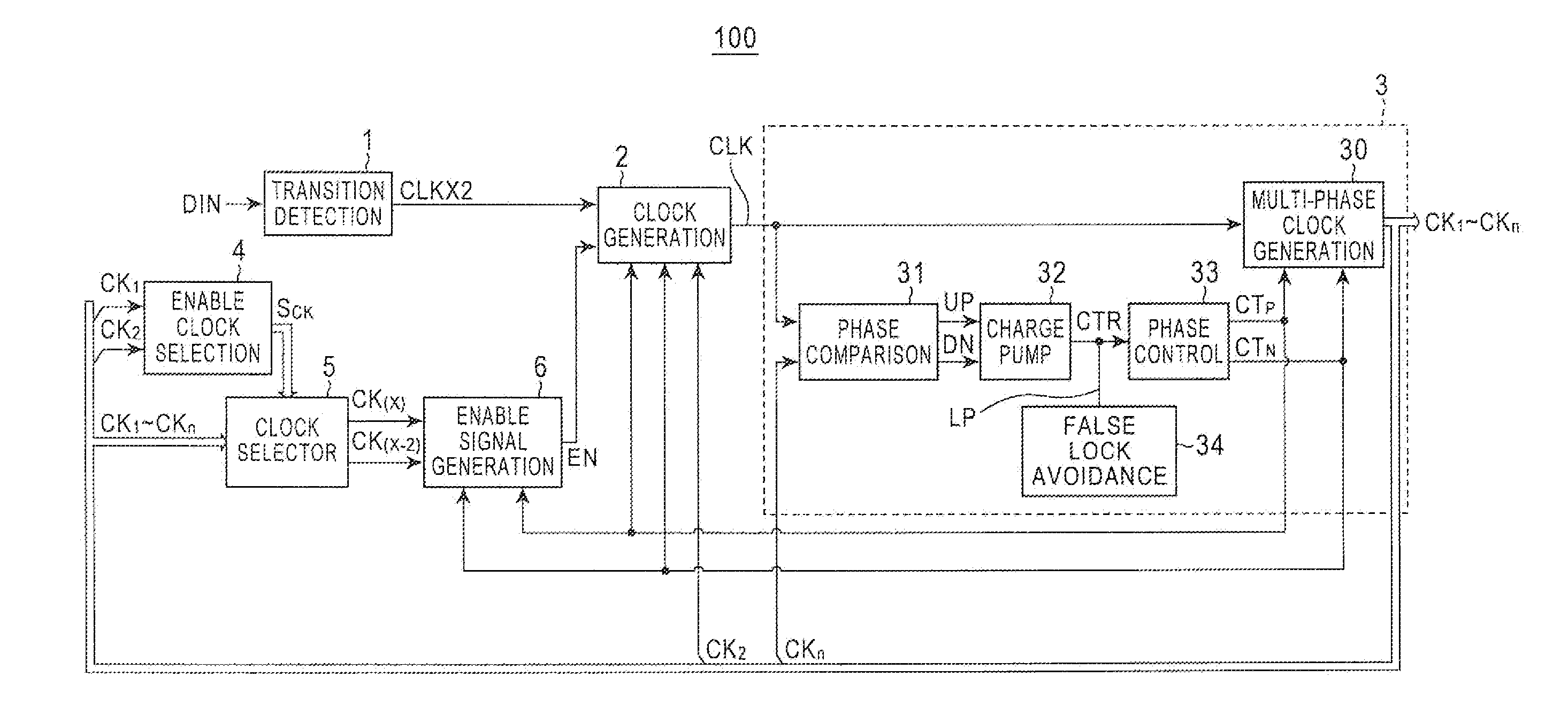
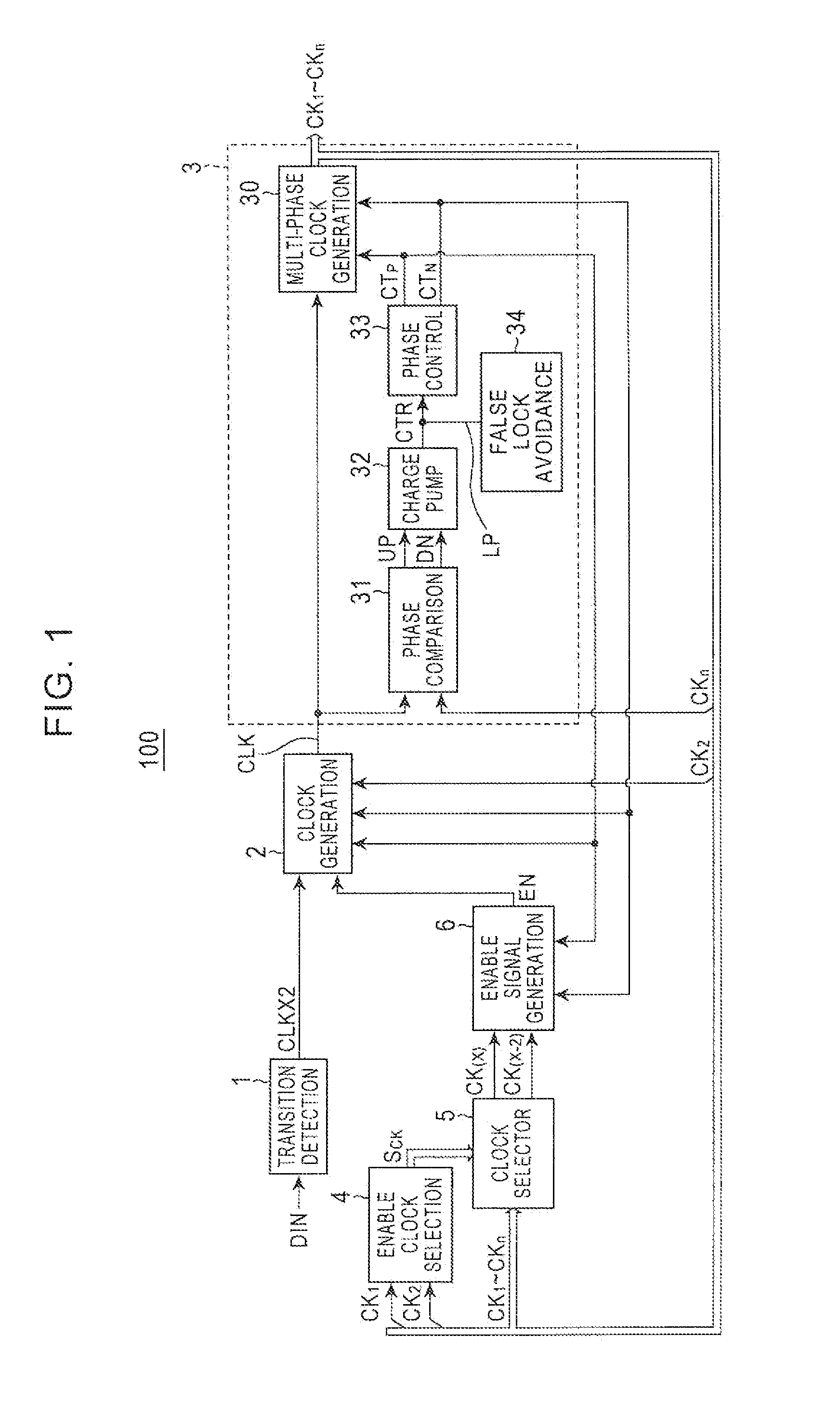
[0028]FIG. 1 is a block diagram illustrating a clock data recovery circuit 100 which includes a DLL circuit 3 serving as a synchronizing circuit according to the present invention.

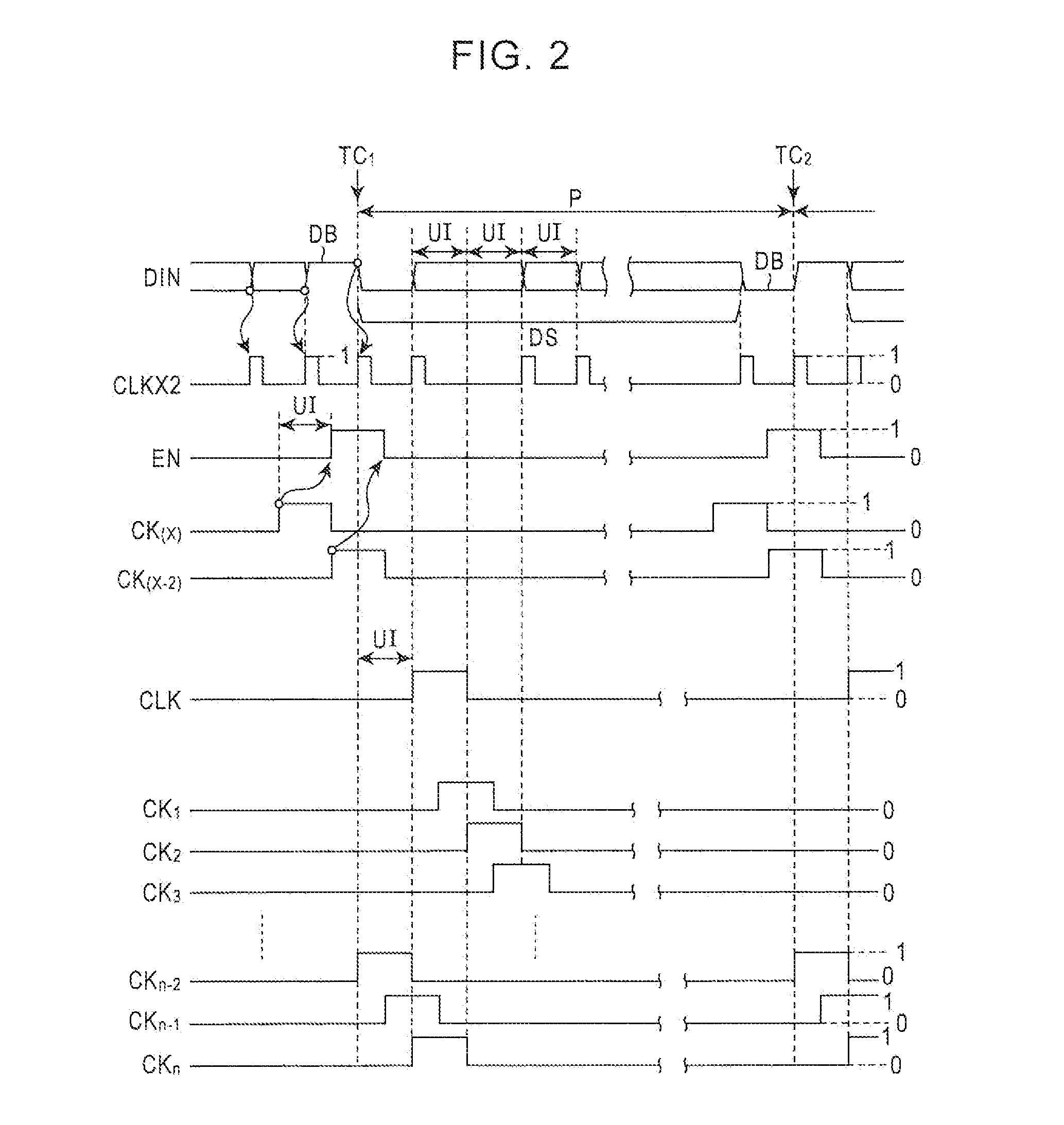
[0029]The clock data recovery circuit 100 shown in FIG. 1 is formed in a semiconductor IC mounted on a receiver device (not shown). Such a receiver receives, demodulates, and binary-codes a transmission signal transmitted by a transmitter (not shown) in order to produce a received data signal DIN. At this time, as shown in FIG. 2, the received data signal DIN has a one-bit dummy bit DB at reference transition periods P inserted into a data train DS of a plurality of data bits each having a unit data period UI. At this time, as shown in FIG. 2, when the leading data bit of the data train DS is at logic level 0, the dummy bit DB at logic level 1 is inserted immediately before the same. On the other hand, when the leading data bit is at logic level 1, the dummy bit DB at logic level 0 is inserted immediately ...


PUM


Abstract

A synchronizing circuit that is capable of generating a reproduced clock signal synchronized with a reference clock signal without causing a false lock and a clock data recovery circuit including the same are provided. To generate a clock signal synchronized with a reference clock signal associated with a data transition point that appears every predetermined period in an input data signal, the following false-lock avoidance processing is performed. That is, precharging of a first line is started when a phase control voltage applied to the first line by a charge pump falls below a lower-limit reference voltage, and the precharging of the first line is continued until the phase control voltage exceeds an upper-limit reference voltage.

Description

BACKGROUND OF THE INVENTION[0001]1. Field of the Invention[0002]The present invention relates to a synchronizing circuit for generating a reproduced clock signal synchronized with a reference clock signal and a clock data recovery circuit (hereinafter to be referred to as a CDR circuit) including the synchronizing circuit.[0003]2. Description of the Related Art[0004]Currently employed as a high-speed serial data communication scheme is an embedded clock scheme in which a clock signal is superimposed on data signals for transmission.[0005]A receiver in a communication system that employs the embedded clock scheme is provided with a CDR circuit for acquiring a reproduced clock signal in phase with a data transition point from a received data signal with the help of the periodicity of data transition of the received data signal (for example, see FIG. 5 in Japanese Patent Application Laid-Open No. 2011-30058). The CDR circuit includes a phase locked loop (PLL) circuit which is made up o...

Claims


Application Information

Patent Timeline
IPC IPC(8): H03L7/085
CPCH03L7/085H03L7/0816H03L2207/14
Inventor NAKAYAMA, AKIRAHARAYAMA, KUNIHIRO
Owner LAPIS SEMICON CO LTD
Why Eureka
Try Eureka