

Phosphorescent compound and organic light emitting diode device using the same
Active Publication Date: 2014-06-05
LG DISPLAY CO LTD
View PDF2 Cites 7 Cited by
- Summary
- Abstract
- Description
- Claims
- Application Information
AI Technical Summary
Benefits of technology
The technical effects of this patent text are to provide an OLED that is more efficient in emitting light.
Problems solved by technology
Method used
View moreImage
Smart ImageViewing Examples

Examples
example
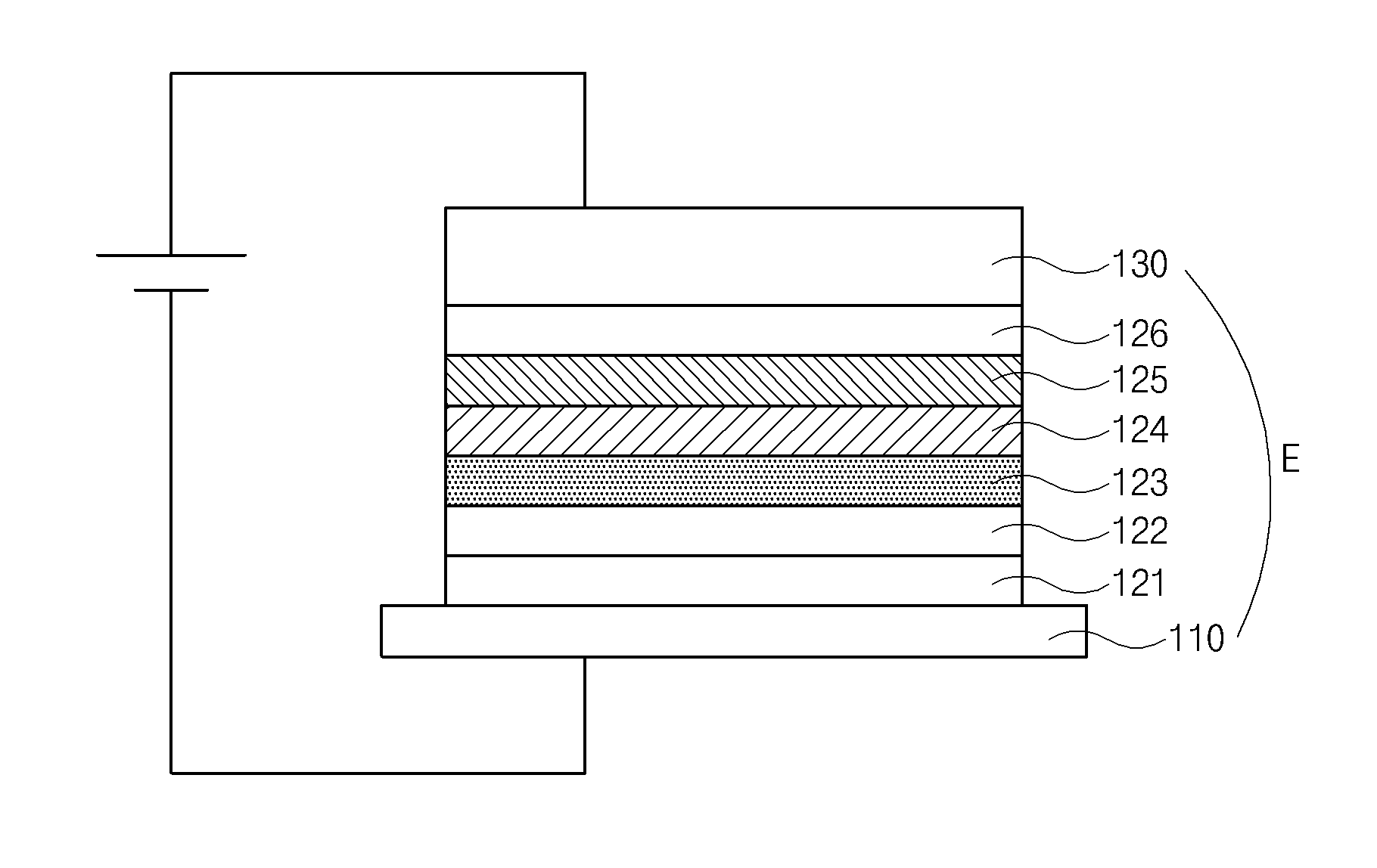
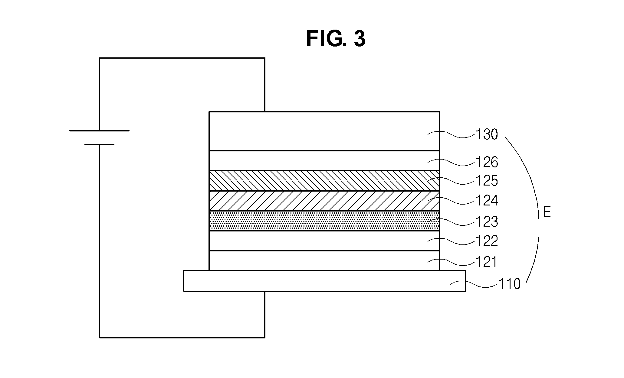
[0044]An ITO layer is deposited and patterned to have an area of 3 mm*3 mm on a substrate and washed to form an anode. The substrate is loaded in a vacuum chamber, and a hole injecting layer (50 Å) of hexaazatriphenylene-hexacarbonitrile (HAT-CN), a hole transporting layer (550 Å) of 4-4′-bis[N-(1-naphtyl)-N-phenylamino]-biphenyl (NPB), an electron blocking layer (100 Å) of di-(4-(N,N′-ditolyl-amino)-phenyl)cyclohexane (TAPC), an emitting material layer (300 Å) of the “A-1” phosphorescent compound in the above Formula 5 and a blue dopant (15%) of FCNIr, an electron transporting layer (400 Å) of TmPyPB, an electron injecting layer (5 Å) of LiF, and a cathode (1100 Å) of aluminum are sequentially formed on the anode.
Login to View More PUM
 Abstract
The present invention provides a phosphorescent compound of following formula:wherein each of X1 and X2 is independently selected from substituted or non-substituted carboline, dibenzofuran, dibenzothiophene and fluorene.
Description
[0001]The present application claims the benefit of Korean Patent Application No. 10-2012-0138993 filed in Korea on Dec. 3, 2012, which is herein incorporated by reference.BACKGROUND OF THE INVENTION[0002]1. Field of the Invention[0003]The present invention relates to a phosphorescent compound and an organic light emitting diode (OLED) device and more particularly to a phosphorescent compound having improved emitting efficiency due to high triplet energy and an OLED device using the same.[0004]2. Discussion of the Related Art[0005]Recently, requirement for flat panel display devices having small occupied area is increased. Among the flat panel display devices, an OLED device, which may be called to as an organic electroluminescent device, is widely introduced.[0006]The OLED device emits light by injecting electrons from a cathode as an electron injection electrode and holes from an anode as a hole injection electrode into an emission compound layer, combining the electrons with the ...
Claims
Login to View More Application Information
Patent Timeline
 IPC IPC(8): H01L51/00
CPCC07F7/0814C07F7/10C09K11/06C09K2211/1022C09K2211/1029H10K85/342H10K85/40H10K2102/103C07F7/081
InventorKIM, JUNG-KEUNSONG, IN-BUMSEO, BO-MINYU, JAE-HYUNG
OwnerLG DISPLAY CO LTD