RF testing system

a technology of rf and testing system, which is applied in the direction of transmission monitoring, receiver monitoring, electrical equipment, etc., can solve the problems of increasing cost and time, and challenging problems

Inactive Publication Date: 2014-06-05
MEDIATEK INC
View PDF9 Cites 17 Cited by
  • Summary
  • Abstract
  • Description
  • Claims
  • Application Information

AI Technical Summary

Benefits of technology

This patent describes an integrated circuit (IC) that can communicate with test equipment and perform signal conversion to generate an evaluation signal for testing. The test equipment can then analyze the evaluation signal to determine the test result. This allows for more efficient and accurate testing of RF signals. The technical effect is improved efficiency and accuracy in RF testing.

Problems solved by technology

Due to the increasing complexity of the testing of integrated RF circuits, to identify the “good” and “bad” ICs during production is a challenging problem for those conducting the wafer-level test or final test.
In the traditional testing of RF circuits, what is used is expensive automatic test equipment (ATE), such as UltraFlex or Flex with RF instruments, or equipment used in mixing signals is used for generating an RF test signal (or RF patterns) to a device under test (DUT) and processing RF signals emanating from the DUT, leading to increased cost and time to conduct the tests.

Method used


Image

  • RF testing system
  • RF testing system
  • RF testing system

Examples


Embodiment Construction

[0029]The following description is of the best-contemplated mode of carrying out the invention. This description is made for the purpose of illustrating the general principles of the invention and should not be taken in a limiting sense. The scope of the invention is best determined by reference to the appended claims.

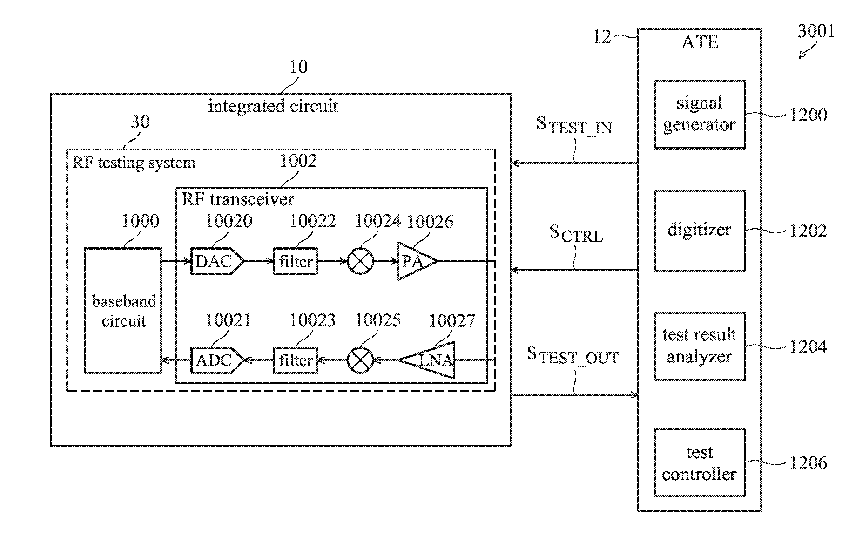
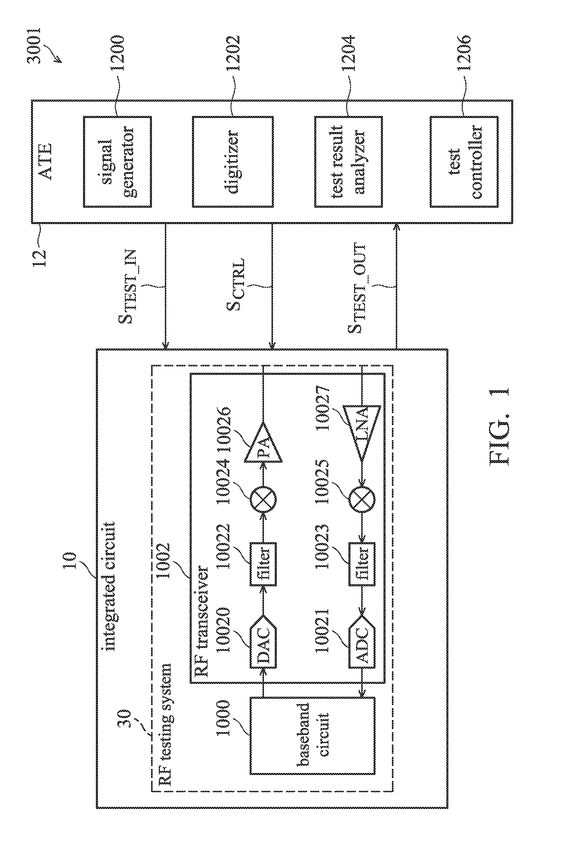
[0030]FIG. 1 is a block diagram of a conventional radio frequency (RF) testing system 3001. As illustrated in FIG. 1, the RF testing system 3001 comprises an integration circuit (IC) 10 and automatic test equipment (ATE) 12. The ATE 12 applies semiconductor testing for digital and analog elements in the IC 10 during the hardware manufacturing procedure. The IC 10 is a device under test (DUT) that receives power and testing patterns from the ATE 12 and outputs testing responses to the ATE 12. The ATE 12 is an electronic apparatus that receives a test program and performs tests accordingly on the DUT by supplying stimulus signals. The ATE 12 also receives outcome signals...


PUM


Abstract

An integrated circuit (IC) is provided. The IC includes an RF transmitter configured to generate an RF signal in response to a command signal from test equipment; an RF receiver configured to generate an evaluation signal according to the RF signal, and report the evaluation signal to the test equipment, so that the test equipment performs a test analysis on the evaluation signal to determine a test result, wherein the test equipment is external to the IC.

Description

CROSS REFERENCE TO RELATED APPLICATIONS[0001]This application claims the benefit of U.S. Provisional Application No. 61 / 731,845, filed at Nov. 30, 2012, the entirety of which is incorporated by reference herein.BACKGROUND OF THE INVENTION[0002]1. Field of the Invention[0003]The present invention relates to semiconductor devices, and in particular to radio frequency (RF) testing systems for semiconductor devices.[0004]2. Description of the Related Art[0005]Semiconductor devices are manufactured in the form of wafers comprising many thousands of devices. The wafers are diced into dies and packaged into integrated circuits (IC). Each IC has been implemented by integrating more and more digital and analog circuits into a single chip.[0006]Due to the increasing complexity of the testing of integrated RF circuits, to identify the “good” and “bad” ICs during production is a challenging problem for those conducting the wafer-level test or final test. In the traditional testing of RF circuit...

Claims


Application Information

Patent Timeline
IPC IPC(8): H04B17/00
CPCH04B17/00H04B17/0085H04B3/46H04B17/29
Inventor CHEN, YEN-LIANGPENG, CHUN-HSIENSHIH, YING-CHOUCHEN, YU-ANYANG, CHUN-WEI
Owner MEDIATEK INC
Why Eureka
Try Eureka