
Light-emitting device

Active Publication Date: 2014-06-12
GENESIS PHOTONICS +1
View PDF4 Cites 0 Cited by
  • Summary
  • Abstract
  • Description
  • Claims
  • Application Information

AI Technical Summary

Benefits of technology

The invention is a light-emitting device that includes a coarse structure on the substrate's side surface. This structure helps scatter the light emitted from the device, preventing total reflection and improving the overall efficiency of the device.

Problems solved by technology

Consequently, the light emitted at the side surfaces of the light-emitting diode cannot be effectively utilized, thereby affecting the light emitting efficiency at the side surfaces of the light-emitting diode and reducing the light-emitting brightness of the light-emitting diode.

Method used


Image

  • Light-emitting device
  • Light-emitting device
  • Light-emitting device

Examples


Embodiment Construction

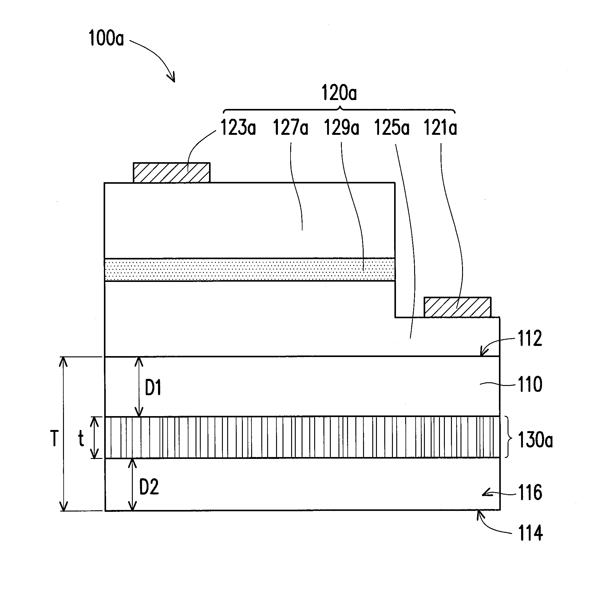
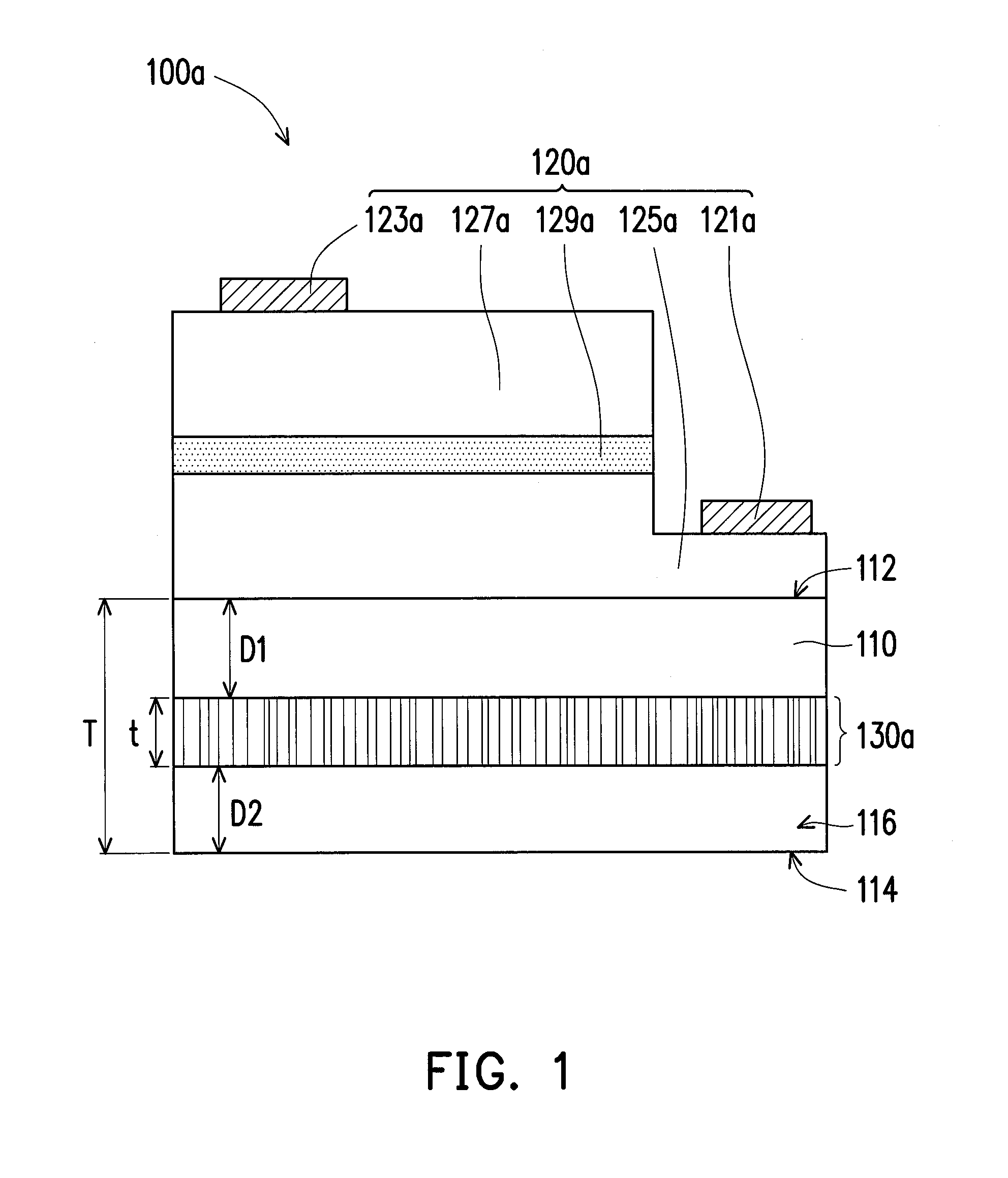
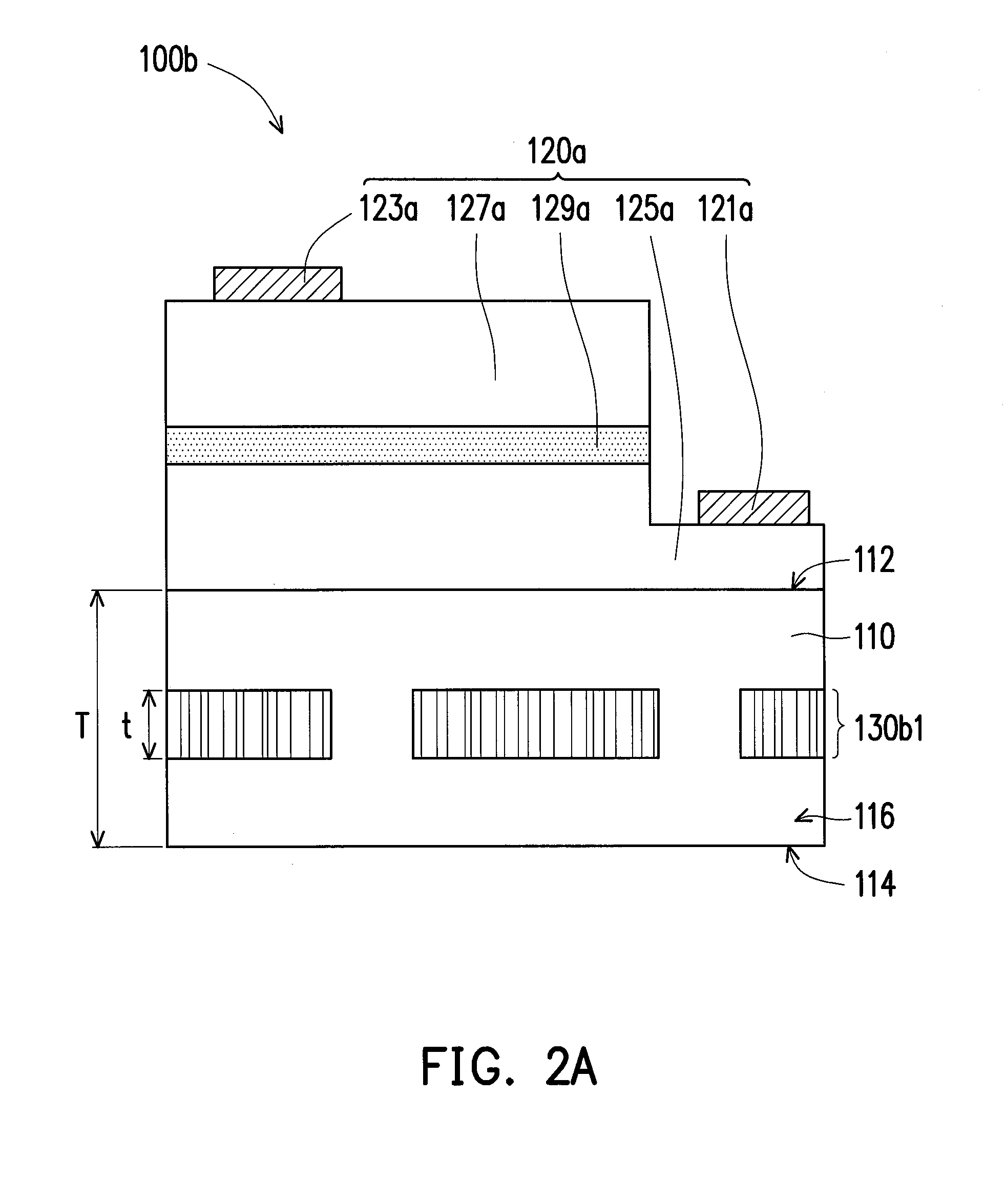
[0030]FIG. 1 is a schematic view of a light-emitting device according to an embodiment of the invention. Referring to FIG. 1, in the embodiment, the light-emitting device 100a includes a substrate 110, a photoelectric structure 120a and a coarse structure 130a. The substrate 110 has an upper surface 112 and a lower surface 114 opposite to each other and an annular side surface 116 connecting the upper surface 112 and the lower surface 114. The photoelectric structure 120a is disposed on the upper surface 112 of the substrate 110. The coarse structure 130a is formed on the annular side surface 116 of the substrate 110. In particular, a ratio of a thickness T of the substrate 110 and a thickness t of the coarse structure 130a is, for example, greater than or equal to 1 and less than or equal to 20.

[0031]More particularly, the photoelectric structure 120a is formed by a first electrode 121a, a second electrode 123a, a first type semiconductor layer 125a, a second type semiconductor lay...


PUM


Abstract

A light-emitting device including a substrate, a photoelectric structure and a coarse structure is provided. The substrate has an upper surface and a lower surface opposite to each other, and an annular side surface connecting the upper surface and the lower surface. The photoelectric structure is disposed on the upper surface of the substrate. The coarse structure is formed on the annular side surface of the substrate. A ratio of a thickness of the substrate and a thickness of the coarse structure is greater than or equal to 1 and less than or equal to 20. Therefore, the overall light-emitting efficiency of the light-emitting device may be improved.

Description

CROSS-REFERENCE TO RELATED APPLICATION[0001]This application claims the priority benefit of Taiwan application Ser. No. 101145826, filed on Dec. 6, 2012. The entirety of the above-mentioned patent application is hereby incorporated by reference herein and made a part of this specification.BACKGROUND OF THE INVENTION[0002]1. Field of the Invention[0003]The invention relates to a light-emitting device, and more particularly relates to a light-emitting device capable of improving the light-emitting efficiency.[0004]2. Description of Related Art[0005]In general, a light-emitting diode wafer usually is fabricated by following steps: providing a substrate, forming an epitaxial structure on the substrate by epitaxial growth, and then disposing electrodes on the epitaxial structure to provide electric power, so that the light-emitting diode wafer may emit light by photoelectric effect. Thereafter, a plurality of scribe lines crisscrossing to each other is formed on the epitaxial structure b...

Claims


Application Information

Patent Timeline
IPC IPC(8): H01L33/22
CPCH01L33/22
Inventor HUANG, YI-RUHUANG, JING-ENWU, CHIH-LINGLO, YU-YUN
Owner GENESIS PHOTONICS
Learn More