Semiconductor lead frame package and LED package
- Summary
- Abstract
- Description
- Claims
- Application Information
AI Technical Summary
Benefits of technology
Problems solved by technology
Method used
Image


Examples
Embodiment Construction
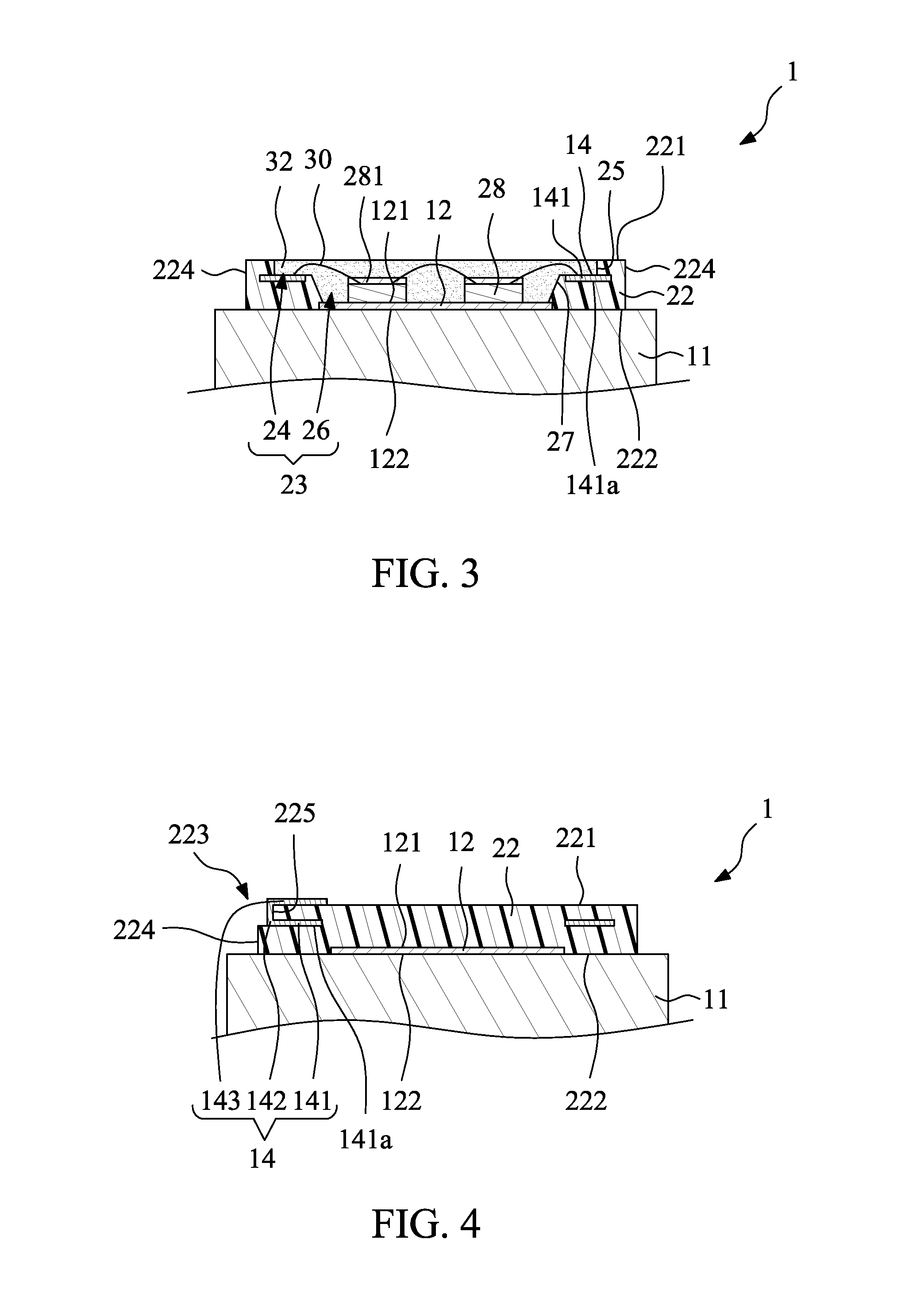
[0024]Referring to FIG. 1, a semiconductor lead frame package 1 according to one embodiment is illustrated. The semiconductor lead frame package 1 includes a die pad 12, at least one lead 14, e.g., two leads 14, at least one rib 16, e.g., four ribs 16, at least one fixing element 18, e.g., two fixing elements 18, an insulator body 22, at least one bonding wire 30, e.g., three bonding wires 30, at least one die 28, e.g., two dies 28, at least one light converting layer 281, e.g., two light converting layers 281, and an encapsulant 32.
[0025]The die pad 12 is used for carrying the die 28. In this embodiment, the die 28 is a light-emitting diode (LED) die, and is adhered to the die pad 12. Thus, the semiconductor lead frame package 1 is a LED package. The material of the die pad 12 is metal such as copper.
[0026]Although two dies 28 are illustrated in the figures, in another embodiment, the semiconductor lead frame package 1 includes only a single die 28. In yet another embodiment, the s...
PUM
 Abstract
Description
Claims
Application Information
 - R&D
- Intellectual Property
- Life Sciences
- Materials
- Tech Scout
- Unparalleled Data Quality
- Higher Quality Content
- 60% Fewer Hallucinations
Browse by: Latest US Patents, China's latest patents, Technical Efficacy Thesaurus, Application Domain, Technology Topic, Popular Technical Reports.
© 2025 PatSnap. All rights reserved.Legal|Privacy policy|Modern Slavery Act Transparency Statement|Sitemap|About US| Contact US: help@patsnap.com