Touch panel and fabrication method thereof

a technology of touch panel and fabrication method, which is applied in the direction of superimposed coating process, liquid/solution decomposition chemical coating, instruments, etc., can solve the problems of unsatisfactory appearance effect, uneasy cleaning of touch panel, and inferior reliability, so as to improve reliability and simplicity, maintain the appearance of touch panel, and facilitate cleaning

Active Publication Date: 2014-06-26
TPK TOUCH SOLUTIONS (XIAMEN) INC
View PDF1 Cites 8 Cited by
  • Summary
  • Abstract
  • Description
  • Claims
  • Application Information

AI Technical Summary

Benefits of technology

[0010]The touch panel and the fabrication method of the touch panel, provided in the present disclosure, include disposing electrode arrays corresponding to both the display region. and the peripheral region of touch panel so as to possess their respective touch response functions. Therefore, there is no need of any through holes designed on the surface of the touch panel to keep the evenness of the touch panel appearance with easy cleaning. Moreover, the electrode arrays used for actualizing various touch response functions can be finished in the same step of manufacturing process to empower the touch panel in this disclosure with more reliability and simplicity.

Problems solved by technology

Moreover, as the current design of electronics is oriented towards being light-weight, thin, brief, and compact, there exists insufficient space in products for containing traditional input devices such as keyboard, mouse etc., and especially under the driving impact of the need for tablet PCs, touch panels have become one of the key components.
However, the traditional physical button can only be used by designing through holes on the surface of the touch panel, which leads to relatively undesirable appearance effect, inferior reliability, and uneasy cleaning of touch panels.
Moreover, the physical button requires another step of assembling, and therefore the fabrication process is complex.

Method used


Image

  • Touch panel and fabrication method thereof
  • Touch panel and fabrication method thereof
  • Touch panel and fabrication method thereof

Examples


Embodiment Construction

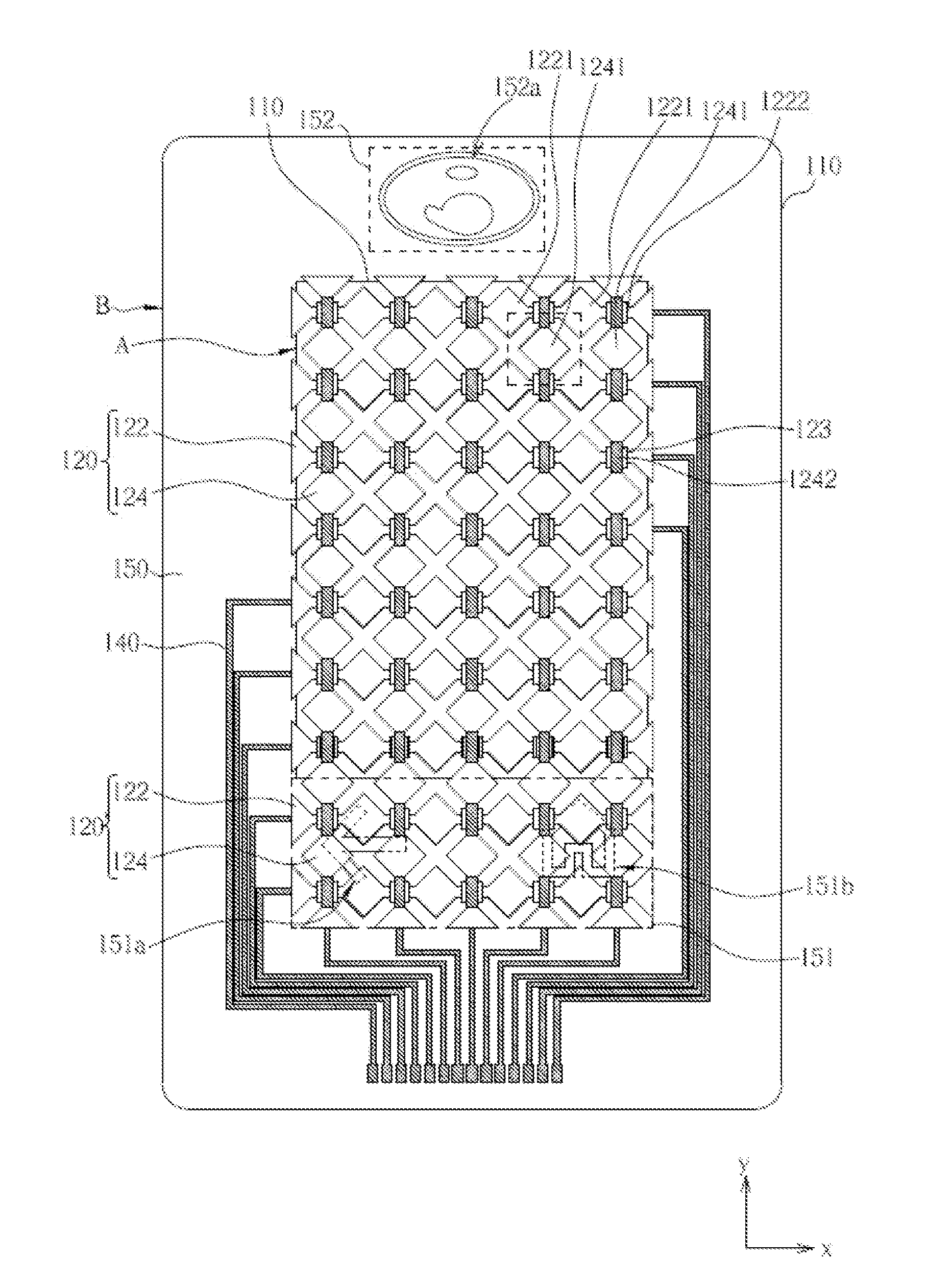
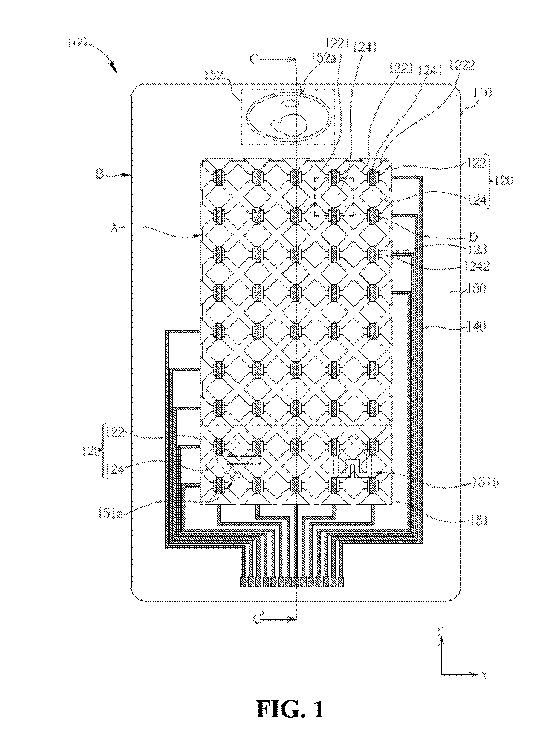
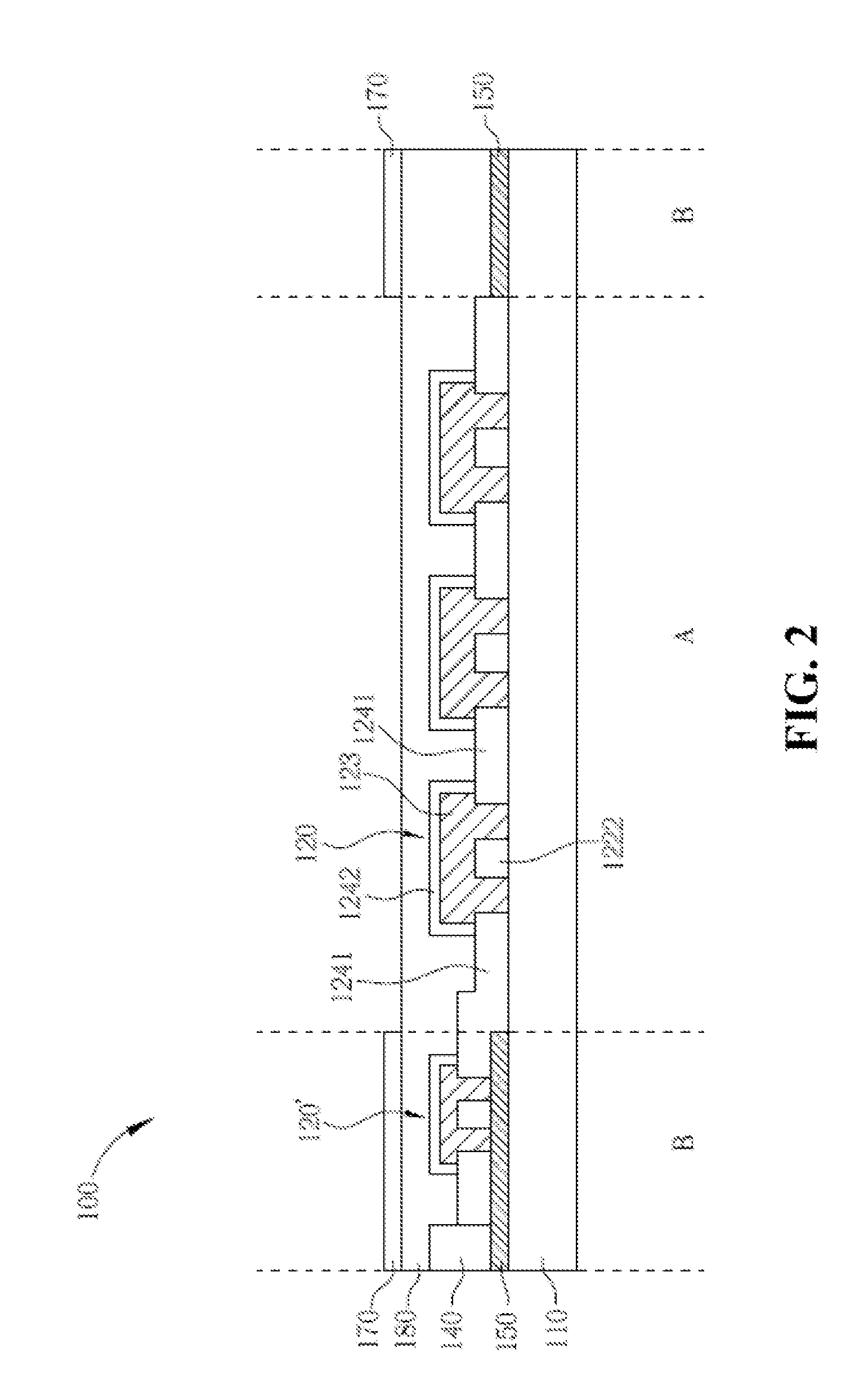
[0017]FIG. 1 shows top view of a touch panel in accordance with an embodiment of the present disclosure, wherein the touch panel 100 can be applied to electronic devices with screen display function such as computer, mobile phone, acoustic equipment and vehicle-used apparatus. The touch panel 100 in the present embodiment is illustrated from an overlooking angle of the reverse side, which is also described as the untouched surface for the user when the touch panel 100 is made into use. As shown in FIG. 1, the touch panel 100 comprises an upper cover substrate 110. a first electrode array 120, at least one second electrode array 120′, and a patterned mask layer 150.

[0018]The upper cover substrate 110 comprises a display region A and a peripheral region B, wherein the peripheral region B surrounds the display region A. Specifically, the screen visible area of the foregoing electronic device is one that is disposed on the display region A, While the patterned mask layer 150 is disposed...


PUM

PropertyMeasurementUnit
conductiveaaaaaaaaaa
weightaaaaaaaaaa
areaaaaaaaaaaa

Abstract

The present disclosure relates to a touch panel, and more particularly, to a kind of touch panel which actualizes various touch response functions on a same surface and a fabrication method thereof. The touch panel includes an upper cover substrate, a first electrode array, a patterned mask layer, and at least a second electrode array. The upper cover substrate includes a display area and a peripheral area surrounding the display area. The first electrode array is disposed corresponding to the display area. The patterned mask layer is disposed corresponding to the peripheral area. At least a second electrode array is disposed corresponding to a first patterned area of the patterned mask layer. A fabricating method for the touch panel is also provided.

Description

BACKGROUND OF THE INVENTION[0001]This Application claims the benefit of the People's Republic of China Application No. 201110455694.4, filed on Dec. 25, 2011.[0002]1. Field of the Invention[0003]The present disclosure relates to a touch technique, and more particularly to a touch panel and a fabrication method thereof.[0004]2. Description of the Related Art[0005]In the current market for various consumer electronics, touch panels are widely used as a human interface in the portable electronics such as personal digital assistant, mobile phone, notebook, and tablet PC. Moreover, as the current design of electronics is oriented towards being light-weight, thin, brief, and compact, there exists insufficient space in products for containing traditional input devices such as keyboard, mouse etc., and especially under the driving impact of the need for tablet PCs, touch panels have become one of the key components.[0006]The area of the current touch panel can roughly be divided into the di...

Claims


Application Information

Patent Timeline
Patent Type & Authority Applications(United States)
IPC IPC(8): H05K1/02H05K3/10
CPCH05K3/108H05K1/0296G06F3/0443G06F3/0446G06F2203/04103G06F2203/04111
Inventor JIANG, YAU-CHENWU, JIACAI, ZHIXIONGHUANG, PINGPING
Owner TPK TOUCH SOLUTIONS (XIAMEN) INC
Why Eureka
Try Eureka