Light source, exposure apparatus, image display unit and medical device

Inactive Publication Date: 2007-01-04
FUJIFILM CORP
View PDF6 Cites 9 Cited by
  • Summary
  • Abstract
  • Description
  • Claims
  • Application Information

AI Technical Summary

Benefits of technology

[0044] In an embodiment of the invention, the negative electrode has a laminated structure, and the laminated structure comprises an aluminum layer and a silver layer, or an aluminum layer and a copper layer, provided in the above order from the side of the organic compound layer. When the negative electrode is of the aluminum layer and the silver layer, or the aluminum layer and the copper layer, each of these layers preferably has a film thickness as follows. Note that, in the aluminum layer and the silver layer or the aluminum layer and the copper layer, impurities of an inorganic material and / or an organic material may be contained to a degree that the advantage of the invention is not lowered. The aluminum layer is a layer of which main component is aluminum, and preferably, it is a layer only composed of aluminum. The silver layer is a layer of which main component is silver, and preferably, it is a layer only composed of silver. The copper layer is a layer of which main component is copper, and preferably, it is a layer only composed of copper.
[0045] The film thickness of the aluminum layer is preferably 0.01 μm to 0.05 μm so as to keep the evenness of the film.
[0046] From the viewpoint of preventing the voltage drop, it is preferable that the film thickness of the silver layer or the copper layer is 0.4 μm to 2.0 μm, and more preferably, 0.6 μm to 1.5 μm.
[0047] In an embodiment of the laminated structure of the organic compound layer in the invention, a positive hole transport layer, a light emitting layer, and an electron transport layer are formed in this order from the positive electrode side. Further, a charge blocking layer or the like may be disposed between the positive hole transport layer and the light emitting layer, or between the light emitting layer and the electron transport layer. A positive hole injection layer may be disposed between the positive electrode and the positive hole transport layer, and an electron injection layer may be disposed between the negative electrode and the electron transport layer. In addition, the light emitting layer may be one layer or the light emitting layer may be divided into a first light emitting layer, a second light emitting layer, and a third light emitting layer. Further, each layer may be further divided into plural second layers.
[0048] The light emitting layer may receive the positive hole from the positive electrode, the positive hole injection layer, or the positive hole transport layer upon application of the electric field and receive the electron from the negative electrode, electron injection layer or the electron transport layer, thereby providing a filed where the positive hole is recombined to the electron so as to emit a light.
[0049] The light emitting layer in the invention may be composing of only a luminescence material or it may be composed of a mixed layer having a host material and a luminescence material mixed therein. The luminescence material may be a fluorescence material or a phosphorescence material. One luminescence material may be used alone or two or more luminescence materials may be used in combination. The host material is preferably a charge transport material. One host material may be used alone or two or more host materials may be used in combination. Examples thereof include a structure in which a host material with an electron transportability is mixed with a host material with a hole transportability. Further, the light emitting layer may include a material that does not emit a light without the charge transportability.

Problems solved by technology

In a conventional tube, LED or the like used as a light source of an exposure apparatus, the volume of the light source is large, and it is difficult to obtain the evenness of the luminance (spacious and / or positional).
In addition, when using an inorganic EL, it is difficult to obtain a necessary luminance (particularly, in the blue to green regions) and a complicated operational circuit due to alternate current operation and noise suppression are needed.
Therefore, this has a problem that generation of the unevenness of the luminance due to voltage drop is expected.

Method used


Image

  • Light source, exposure apparatus, image display unit and medical device
  • Light source, exposure apparatus, image display unit and medical device
  • Light source, exposure apparatus, image display unit and medical device

Examples


example 1

[0094] A light source of Example 1 is manufactured as follows.

(Structure of Light Source)

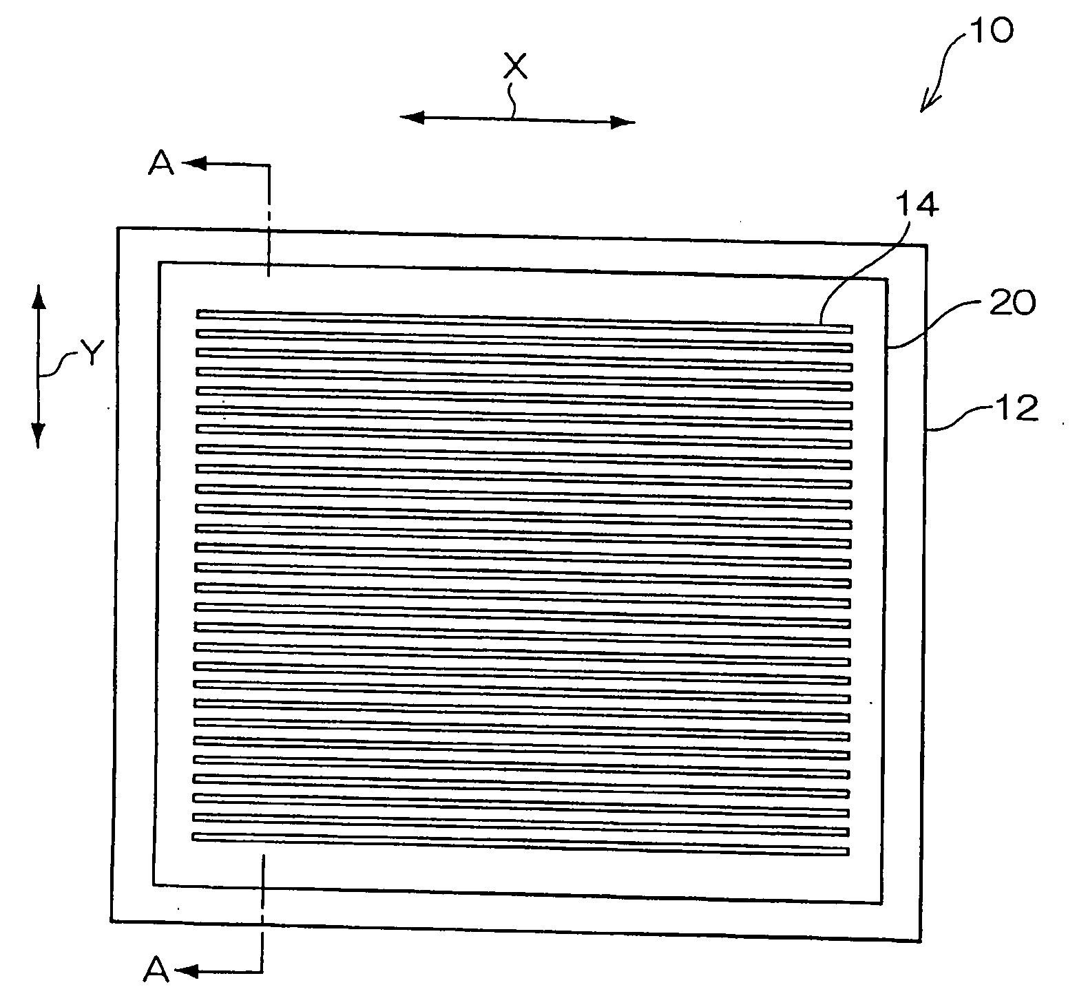
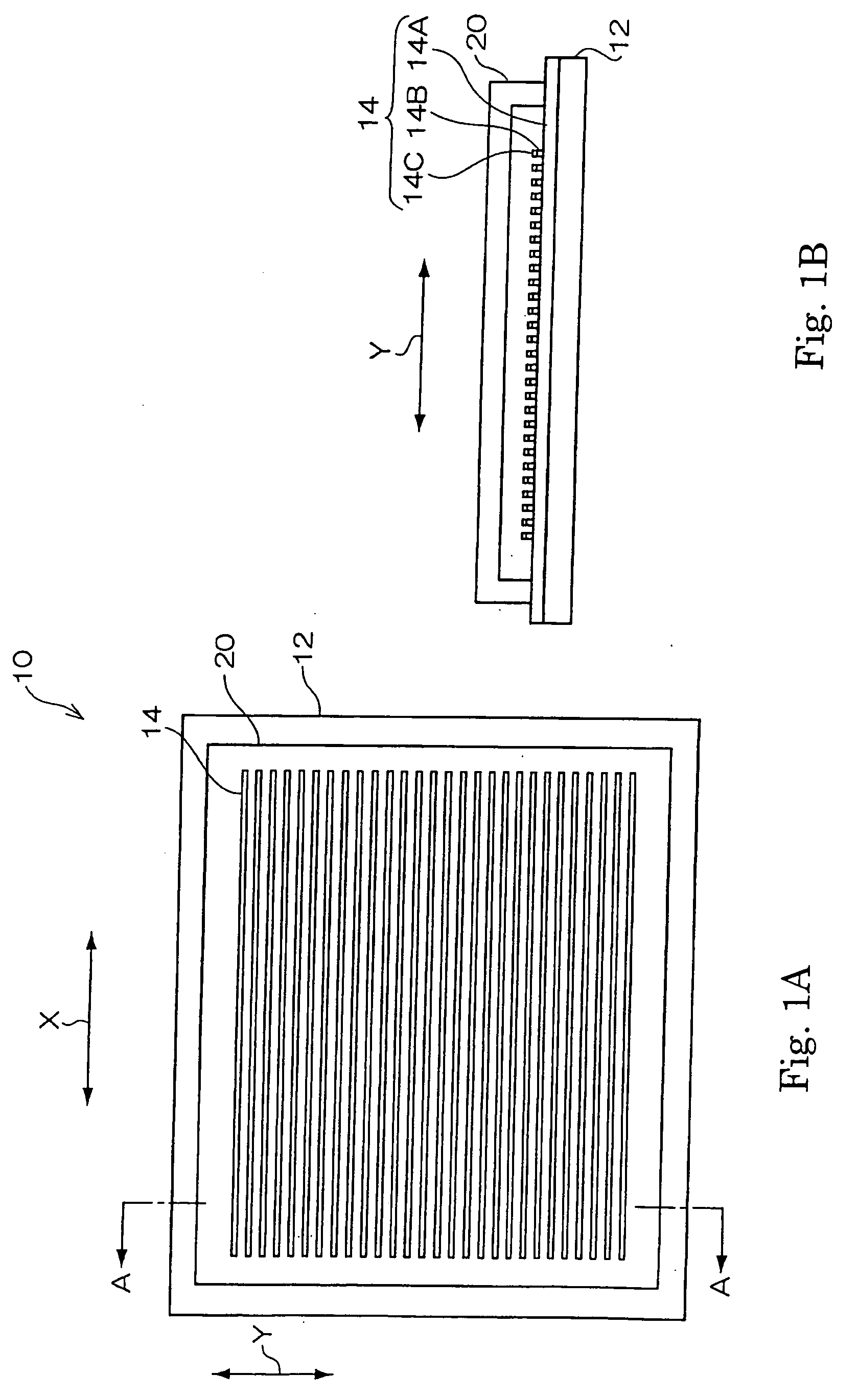
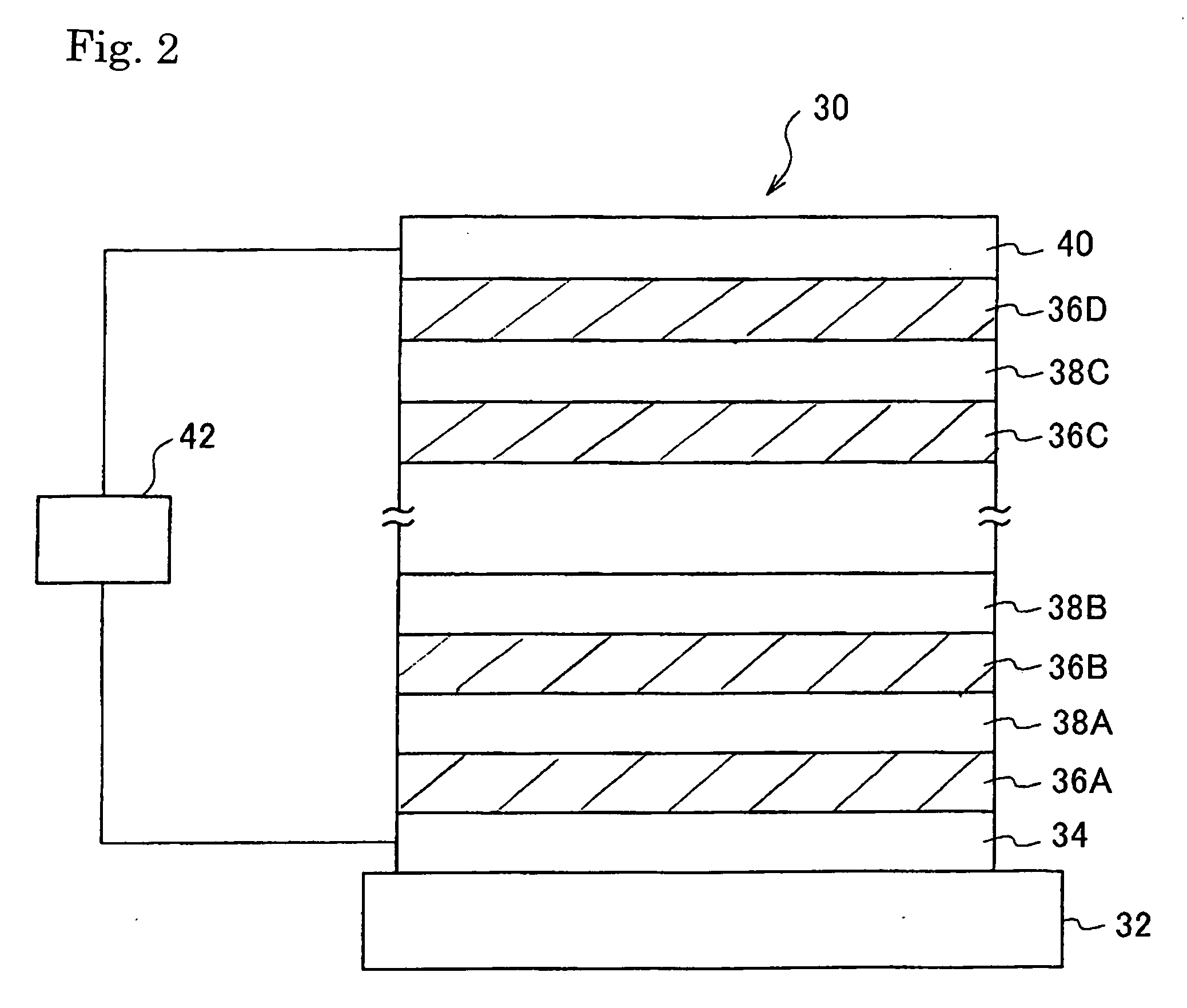
[0095] Size of a linear pixel: 40 cm×50 μm (aspect ratio: 8,000), the number of pixel: 4,000, Pitch: 100 μm, Light emission area: 40 cm×40 cm, Structure of a linear pixel (an organic EL device): ITO / CuPc / NPD / mCP-Firpic (95:5, a mass ratio), a film thickness: 0.1 μm) / Balq / Alq / LiF / Al (a film thickness: 0.4 μm)

(Manufacturing Method)

[0096] On an ITO substrate(a soda glass) of 440×440×0.7 mm, 4001 pieces of dividing walls having a size of 40 cm×50 μm were formed at a pitch of 100 μm. In a pixel area between the diving walls on the substrate, CuPC (10 nm), NPD (30 nm), mCP (95 mass %), Firpic (5 mass %) (100 nm), Balq (10 nm), Alq (40 nm), LiF (0.5 nm), and Al (400 nm) were sequentially deposited according to a resistance heat deposition method. After connecting a lead to a negative electrode of each pixel, the pixel area was sealed by a sealing member having a drying agent.

[0097] Hereinafter, ...

example 2

[0098] Except that the negative electrode of the organic EL device composing the linear pixel was changed into Al (film thickness: 1 μm) in Example 1, a light source of Example 2 was manufactured in the same manner as Example 1.

example 3

[0099] Except that the negative electrode of the organic EL device composing the linear pixel was changed into Al (film thickness: 2 μm) in Example 1, a light source of Example 3 was manufactured in the same manner as Example 1.


PUM


Abstract

To provide a light source including at least two linear pixels arranged in parallel on a substrate, wherein the linear pixels are configured by an organic electroluminescent device having a positive electrode, a negative electrode and at least one organic compound layer containing a light emitting layer between the positive electrode and the negative electrode, wherein an aspect ratio of the linear pixel is 200 or more, the positive electrode is shared by plural linear pixels, and the negative electrode is patterned according to the linear pixels. It is preferable that the film thickness of the negative electrode is 0.4 μm to 2 μm.

Description

CROSS-REFERENCE TO RELATED APPLICATION [0001] This application claims priority under 35 USC 119 from Japanese Patent Application No. 2005-178070, the disclosure of which is incorporated by reference herein. BACKGROUND OF THE INVENTION [0002] 1. Field of the Invention [0003] The present invention relates to a light source having an organic electroluminescent device for converting electric energy into light. Further, the present invention relates to an exposure apparatus, an image display unit, and a medical device having the light source. [0004] 2. Description of Related Art [0005] A light source using an organic electroluminescent (EL) device is known. An organic electroluminescent device has advantages, such as giving light emission of a high luminance under a low voltage, making the device thin, and reduction in size and weight of the device. In a conventional tube, LED or the like used as a light source of an exposure apparatus, the volume of the light source is large, and it is ...

Claims


Application Information

Patent Timeline
IPC IPC(8): H01J1/62
CPCH01L51/5036H01L51/5203H05B33/26H05B33/14H01L2251/5361H10K50/125H10K59/805H10K50/805
Inventor NABETA, TOSHIYUKIHASEGAWA, KAZUHIRO
Owner FUJIFILM CORP
Why Eureka
Try Eureka