Film thickness metrology

a film thickness and metrology technology, applied in the direction of individual semiconductor device testing, semiconductor/solid-state device testing/measurement, instruments, etc., can solve the problems of inability to achieve accuracy, difficult to reliably tease out an accurate film thickness measurement from the scatterometry signal, and the challenge of integrated circuit (ic) chip production

Inactive Publication Date: 2014-07-10
IBM CORP
View PDF1 Cites 2 Cited by
  • Summary
  • Abstract
  • Description
  • Claims
  • Application Information

AI Technical Summary

Problems solved by technology

Integrated circuit (IC) chip production is challenged by complex three-dimensional structures and films associated with these structures.
Moreover, accuracy can only be attained if most or all other parameters are tightly controlled, and measurement devices are calibrated according to the specific set of parameters.
This is due to the complex signature of the reflected signal.
Even with tight control of the features, it remains difficult to reliably tease out an accurate film thickness measurement from the scatterometry signal.
The utility of scatterometry methods are particularly limited in production mode.
However, taking cross sections to perform these techniques is destructive to the IC chip, and therefore substantially incompatible with use in production mode.
It is also slow to perform, and produces a limited quantity of data.

Method used


Image

  • Film thickness metrology
  • Film thickness metrology
  • Film thickness metrology

Examples


Embodiment Construction

[0014]As indicated above, aspects of the invention provide a method for determining a target thickness for a conformal film disposed over at least one three-dimensional feature on an IC chip, as well as an IC chip having a conformal film of a target thickness disposed thereon.

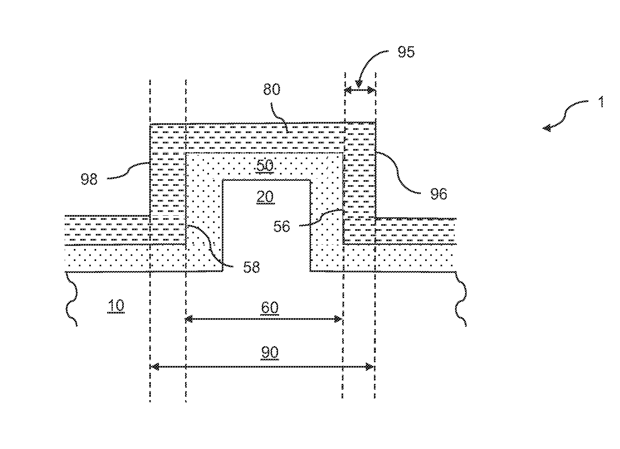
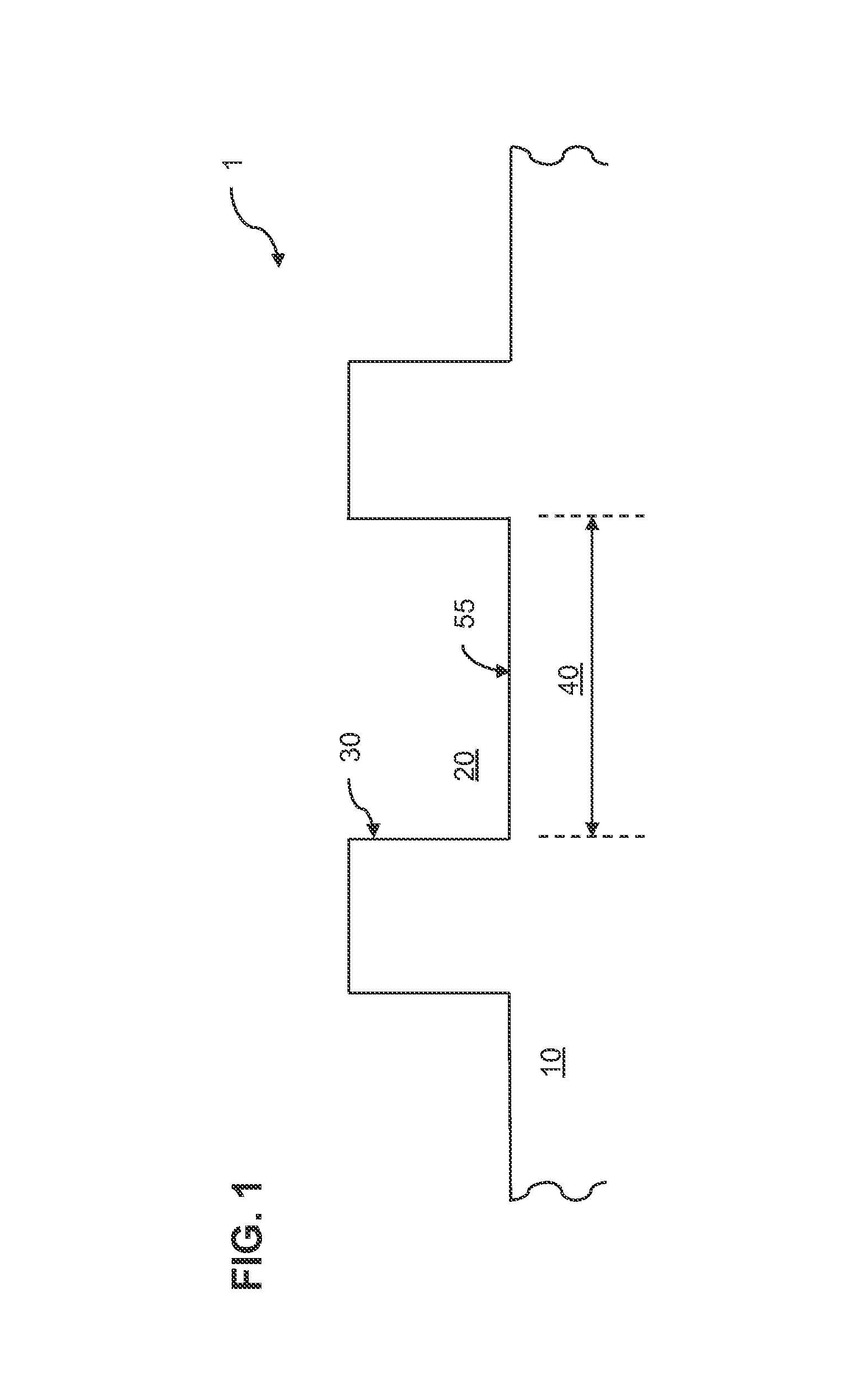
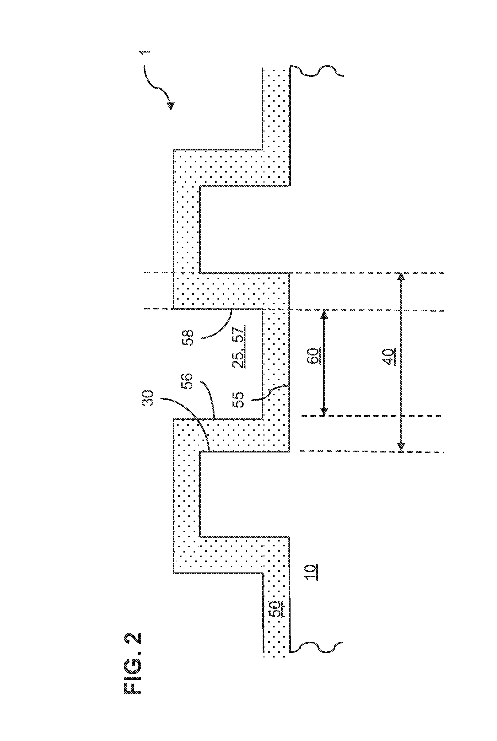
[0015]With reference to FIGS. 1-4, a method of determining the target thickness of a conformal film layer is illustrated. As shown in FIG. 1, an IC chip 1 is provided. IC chip 1 may include a number of electronic circuits manufactured by lithographic processes or patterned diffusion of trace elements into the surface of a wafer 10 in a conventional manner. In particular, a structure 20 having at least one vertical surface 30 and horizontal surface 55 is formed. In FIG. 1, structure 20 is a trench. In other embodiments, however, structure 20 may be a raised feature such as, for example, a fin or a ridge (FIG. 4). In various other embodiments not shown, structure 20 may be any other type of feature which is symme...


PUM


Abstract

Methods for determining a target thickness of a conformal film with reduced uncertainty, and an integrated circuit (IC) chip having a conformal film of the target thickness are provided. In an embodiment, a first critical dimension of a structure disposed on a wafer is measured. Said structure has at least one vertical surface. A first conformal film is deposited over the structure covering each of a horizontal and the vertical surface of the structure. A second critical dimension of the covered structure is then measured. The target thickness of the conformal film is determined based on difference between the first CD measured on the structure and the second CD measured on the covered structure.

Description

FIELD[0001]The disclosure relates generally to production of integrated circuit chips, and more particularly to controlling film thickness on vertical sidewalls of features of IC chips.BACKGROUND[0002]Integrated circuit (IC) chip production is challenged by complex three-dimensional structures and films associated with these structures. Controlling film thickness on sidewalls of vertical surfaces of structures is crucial to proper operation of integrated circuits.[0003]Optical techniques such as scatterometry have been used to assess sidewall film thickness. Scatterometry requires accurate and time-consuming modeling of an entire complex three-dimensional structure in order to achieve accurate measurements of sidewall film thickness. Moreover, accuracy can only be attained if most or all other parameters are tightly controlled, and measurement devices are calibrated according to the specific set of parameters. Such parameters include, for example, the composition of all films, surfa...

Claims


Application Information

Patent Timeline
Patent Type & Authority Applications(United States)
IPC IPC(8): H01L21/66H01L29/06
CPCH01L29/06H01L22/12H01L21/30604H01L22/20H01L27/0203
Inventor STROCCHIA-RIVERA, CARLOS
Owner IBM CORP
Why Eureka
Try Eureka