
High Resolution Organic Light-Emitting Diode Devices, Displays, and Related Methods

Inactive Publication Date: 2014-07-17
KATEEVA
View PDF12 Cites 82 Cited by
  • Summary
  • Abstract
  • Description
  • Claims
  • Application Information

AI Technical Summary

Benefits of technology

The patent text describes a new invention and its features. The invention has various benefits and can be used in different ways without needing all of its features. This allows for flexibility and customization.

Problems solved by technology

Inkjet printing methods can require substantial precision.
Moreover, droplet volumes can be too large with respect to the confinement well and droplets can undesirably spill over into adjacent sub-pixels.
In addition, non-uniformities can form at the edges of the confinement wells due to film drying imperfections.
As the confinement well area is reduced, the non-uniformities can encroach on the active emission area of the pixel creating undesirable visual artifacts in the light emission from the pixel caused by the non-uniformities.
In addition, the ratio of the active area to the total area, both the active and non-active areas, of each pixel (referred to as the “fill factor”) is reduced due to the confinement structures which in turn can reduce the lifetime of the display because each pixel has to be driven using more current to achieve equivalent display brightness levels and using more current to drive each pixel is known to reduce the pixel lifetime.

Method used


Image

  • High Resolution Organic Light-Emitting Diode Devices, Displays, and Related Methods
  • High Resolution Organic Light-Emitting Diode Devices, Displays, and Related Methods
  • High Resolution Organic Light-Emitting Diode Devices, Displays, and Related Methods

Examples


Embodiment Construction

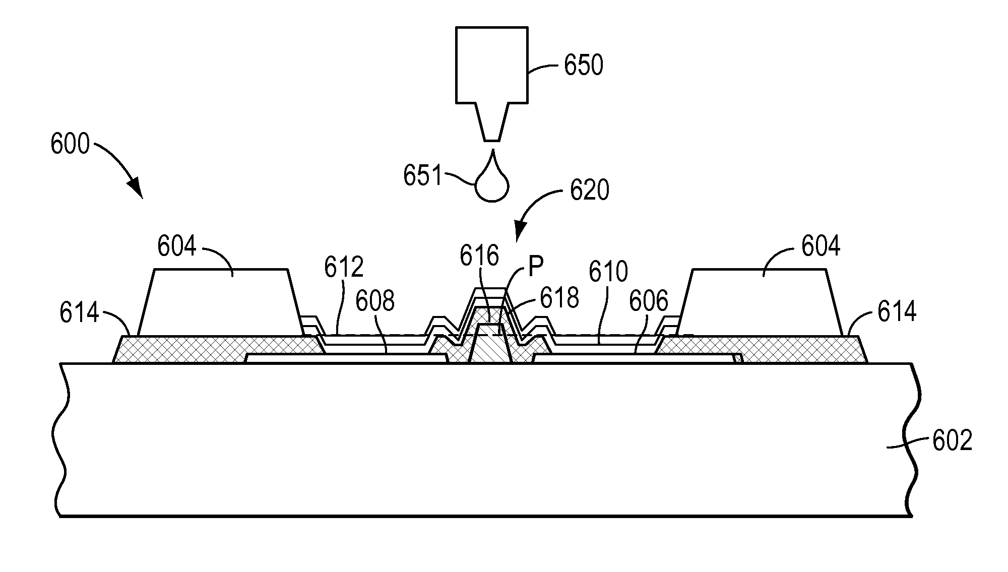
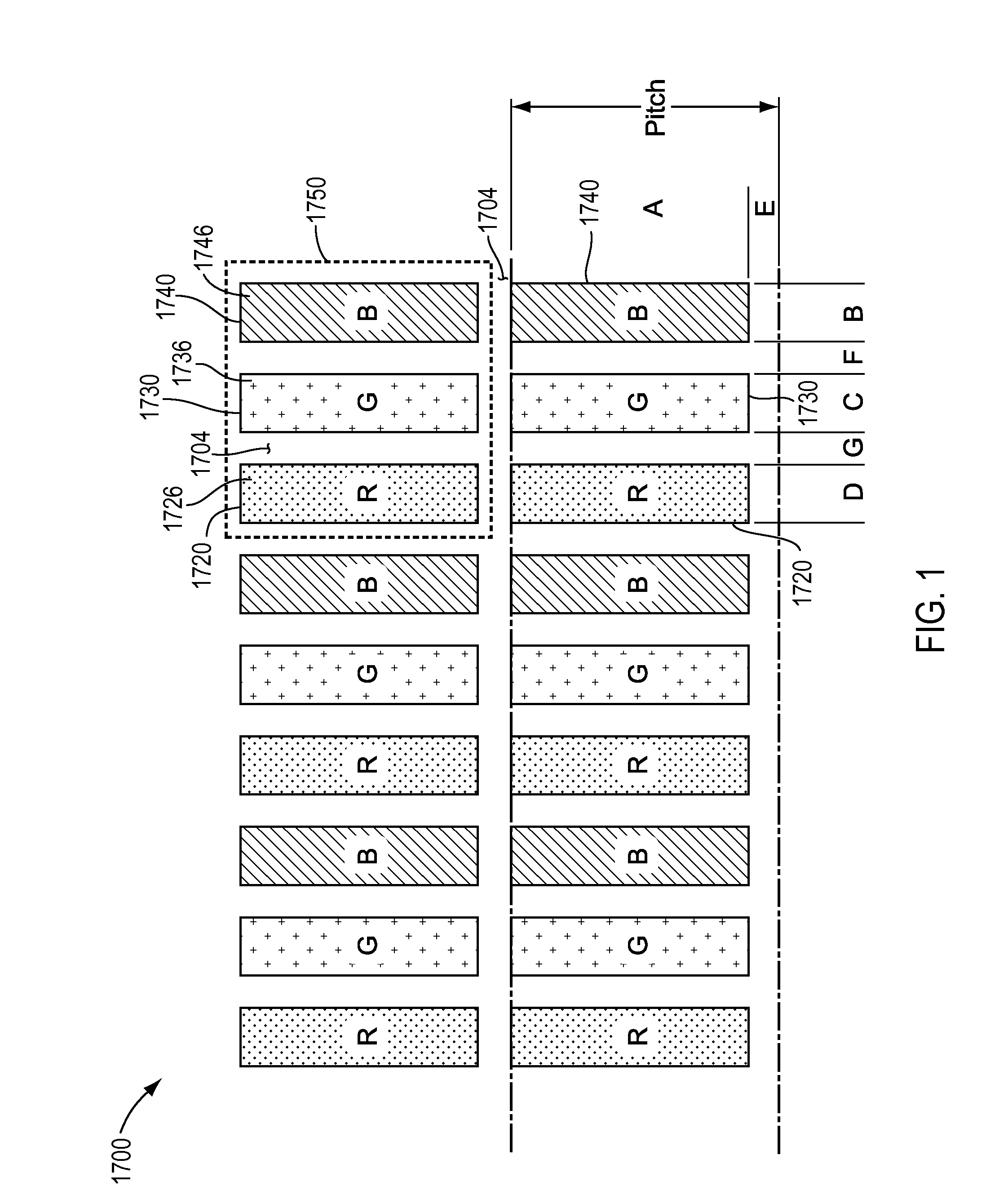
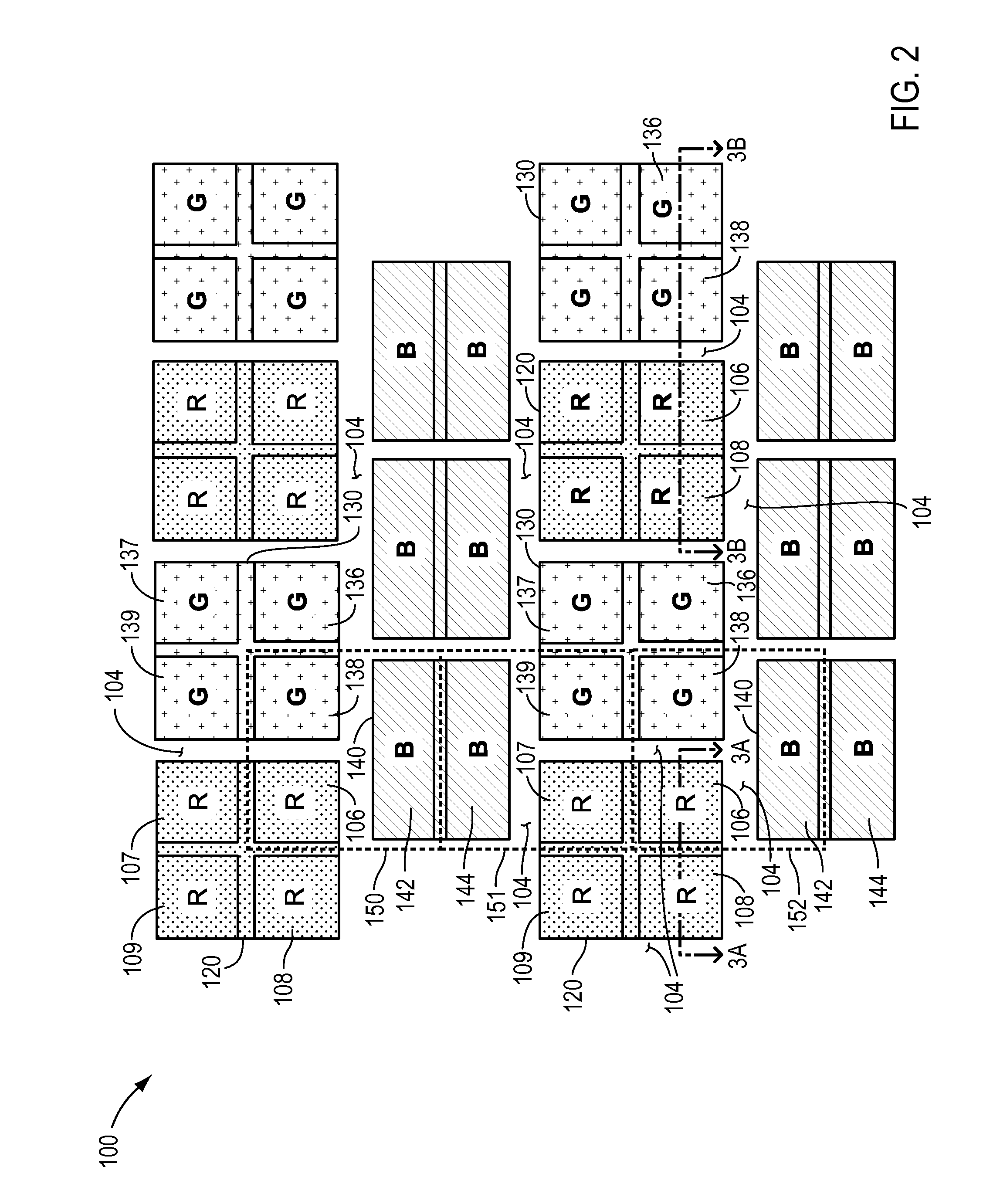
[0027]Reference will now be made in detail to various exemplary embodiments of the present disclosure, examples of which are illustrated in the accompanying drawings. Wherever possible, the same reference numbers will be used throughout the drawings to refer to the same or like parts.

[0028]For the purposes of this specification and appended claims, unless otherwise indicated, all numbers expressing quantities, percentages, or proportions, and other numerical values used in the specification and claims, are to be understood as being modified in all instances by the term “about,” to the extent they are not already so modified. Accordingly, unless indicated to the contrary, the numerical parameters set forth in the following specification and attached claims are approximations that may vary depending upon the desired properties sought to be obtained. At the very least, and not as an attempt to limit the application of the doctrine of equivalents to the scope of the claims, each numeric...


PUM


Abstract

A method of manufacturing an organic-light emitting diode (OLED) display can include providing on a substrate a first electrode associated with a first sub-pixel and a second electrode associated with a second sub-pixel, wherein a gap is formed between the first electrode and the second electrode and wherein the first electrode and the second electrode are positioned in a well having boundaries defined by a confinement structure on the substrate. The method can also include depositing in the well with the electrodes positioned therein, active OLED material to form a substantially continuous layer of active OLED material that spans the boundaries of the well such that a surface of the layer of active OLED material that faces away from the substrate has a non-planar topography. The depositing can be via inkjet printing.

Description

CROSS-REFERENCE TO RELATED APPLICATIONS[0001]This application claims priority to U.S. Provisional Patent Application No. 61 / 753,692, filed Jan. 17, 2013, which is incorporated by reference herein in its entirety.TECHNICAL FIELD[0002]Aspects of the present disclosure generally relate to electronic displays and methods for making electronic displays. More particularly, aspects of the present disclosure relate to depositing organic light-emissive layers on a substrate so as to fabricate high resolution displays.INTRODUCTION[0003]The section headings used herein are for organizational purposes only and are not to be construed as limiting the subject matter described in any way.[0004]Electronic displays are present in many differing kinds of electronic equipment such as, for example, television screens, computer monitors, cell phones, smart phones, tablets, handheld game consoles, etc. One type of electronic display relies on organic light emitting diode (OLED) technology. OLED technolog...

Claims


Application Information

Patent Timeline
IPC IPC(8): H01L51/56H01L51/52
CPCH01L51/5203H01L51/56H10K59/353H10K59/122H10K59/121H10K71/135H10K59/32H10K59/35H10K50/115H10K50/15H10K50/11H10K50/17H10K50/81H10K50/82H10K71/00H10K50/805H10K2102/00H10K2102/103H10K2102/351
Inventor MADIGAN, CONOR FRANCIS
Owner KATEEVA
Features
  • Generate Ideas
  • Intellectual Property
  • Life Sciences
  • Materials
  • Tech Scout
  • Unparalleled Data Quality
  • Higher Quality Content
  • 60% Fewer Hallucinations
Learn More