Topography directed patterning

a topography and patterning technology, applied in the field of integrated circuit fabrication, can solve the problems of prohibitively expensive x-ray and euv lithography implementation, difficulty in forming high-quality reticles, and various technical obstacles

Active Publication Date: 2007-09-27
MICRON TECH INC
View PDF16 Cites 113 Cited by
  • Summary
  • Abstract
  • Description
  • Claims
  • Application Information

AI Technical Summary

Benefits of technology

[0015] According to another aspect of the invention, a partially fabricated integrated circuit is provided. The partially fabricated integrated circuit comprises a plurality of copolymer guides overlying a semiconductor substrate, the guides having a pitch of about 200 nm or less. The partially fabricated integrated circuit also comprises block copolymers disposed between the plurality of copolymer guides.

Problems solved by technology

X-ray and EUV lithography, however, are expected to be prohibitively expensive to implement.
In addition to cost, the techniques face various technical obstacles.
For example, for X-ray lithography, these obstacles include difficulties in forming high quality reticles which are sufficiently opaque to X-rays and difficulties in devising resists which are sufficiently sensitive to the X-rays.
This can cause complications in aligning the reticle with the resist and, in addition, places significant demands on the flatness of both the reticle and the resist.
Similarly, other high resolution lithography techniques, including ion beam and electron beam lithography, have their own technical and practical obstacles, including high complexity and costs.

Method used


Image

  • Topography directed patterning
  • Topography directed patterning
  • Topography directed patterning

Examples


Embodiment Construction

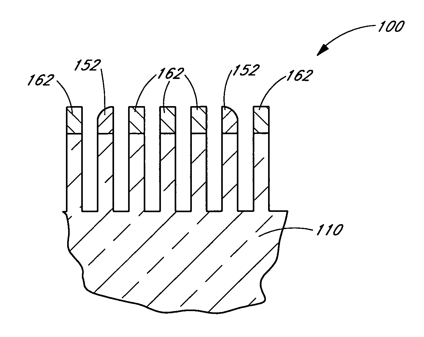
[0042] The ability of block copolymers to self-organize can be used to form mask patterns. Block copolymers are formed of two or more chemically distinct blocks. For example, each block can be formed of a different monomer. The blocks are preferably immiscible or thermodynamically incompatible, e.g., one block can be polar and the other can be non-polar. Due to thermodynamic effects, the copolymers will self-organize in solution to minimize the energy of the system as a whole; typically, this causes copolymers to move relative to one another, e.g., so that like blocks aggregate together, thereby forming alternating regions containing each block type or species. For example, if the copolymers are formed of polar and non-polar blocks, the blocks will segregate so that non-polar blocks aggregate with other non-polar blocks and polar blocks aggregate with other polar blocks. It will be appreciated that the block copolymers may be described as a self-organizing material since the blocks ...


PUM

PropertyMeasurementUnit
thicknessaaaaaaaaaa
thicknessaaaaaaaaaa
thicknessaaaaaaaaaa

Abstract

A pattern having exceptionally small features is formed on a partially fabricated integrated circuit during integrated circuit fabrication. The pattern comprises features formed by self-organizing material, such as diblock copolymers. The organization of the copolymers is directed by spacers which have been formed by a pitch multiplication process in which spacers are formed at the sides of sacrificial mandrels, which are later removed to leave spaced-apart, free-standing spacers. Diblock copolymers, composed of two immiscible block species, are deposited over and in the space between the spacers. The copolymers are made to self-organize, with each block species aggregating with other block species of the same type.

Description

BACKGROUND OF THE INVENTION [0001] 1. Field of the Invention [0002] This invention relates generally to integrated circuit fabrication and, more particularly, to printing techniques. [0003] 2. Description of the Related Art [0004] As a consequence of many factors, including demand for increased portability, computing power, memory capacity and energy efficiency, integrated circuits are continuously being made more dense. The sizes of the constituent features, e.g., electrical devices and interconnect lines, that form the integrated circuits are constantly being decreased to facilitate this scaling. [0005] The trend of decreasing feature size is evident, for example, in memory circuits or devices such as dynamic random access memories (DRAMs), flash memory, static random access memories (SRAMs), ferroelectric (FE) memories, etc. To take one example, DRAM typically comprises millions of identical circuit elements, known as memory cells. In general, a capacitor-based memory cell, such ...

Claims


Application Information

Patent Timeline
Patent Type & Authority Applications(United States)
IPC IPC(8): H01L21/311H01L29/04
CPCH01L21/0332H01L21/0337H01L21/0338Y10T428/24058H01L21/3086H01L21/3088Y10T428/2995H01L21/3081G03F7/0002
Inventor SANDHU, GURTEJ S.
Owner MICRON TECH INC
Why Eureka
Try Eureka