Precise current source circuit for bias supply of RF MMIC gain block amplifier application

a current source circuit and amplifier technology, applied in amplifiers, amplifiers with semiconductor devices/discharge tubes, electrical devices, etc., can solve the problems of overdrive of final stage amplifiers, damage to final stage amplifiers, and increase the margins of mmic amplifier output power capability, so as to reduce the bias voltage (vbias) and operation current

Inactive Publication Date: 2014-07-17
MICROELECTRONICS TECH INC
View PDF2 Cites 3 Cited by
  • Summary
  • Abstract
  • Description
  • Claims
  • Application Information

AI Technical Summary

Benefits of technology

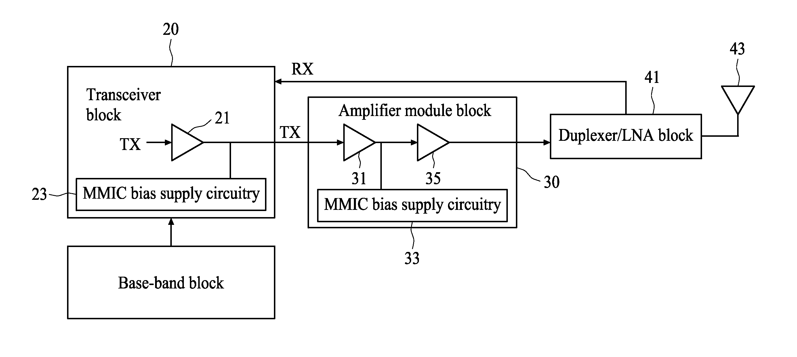
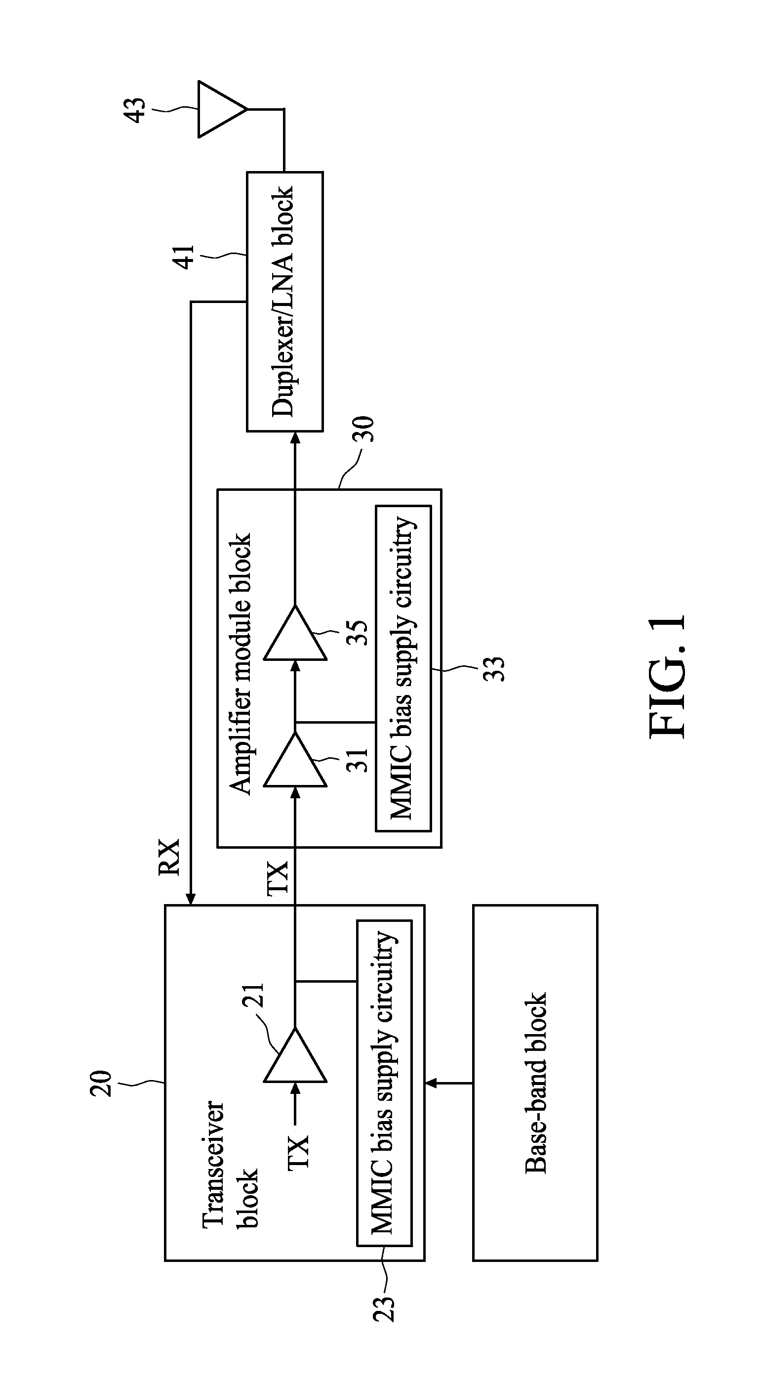
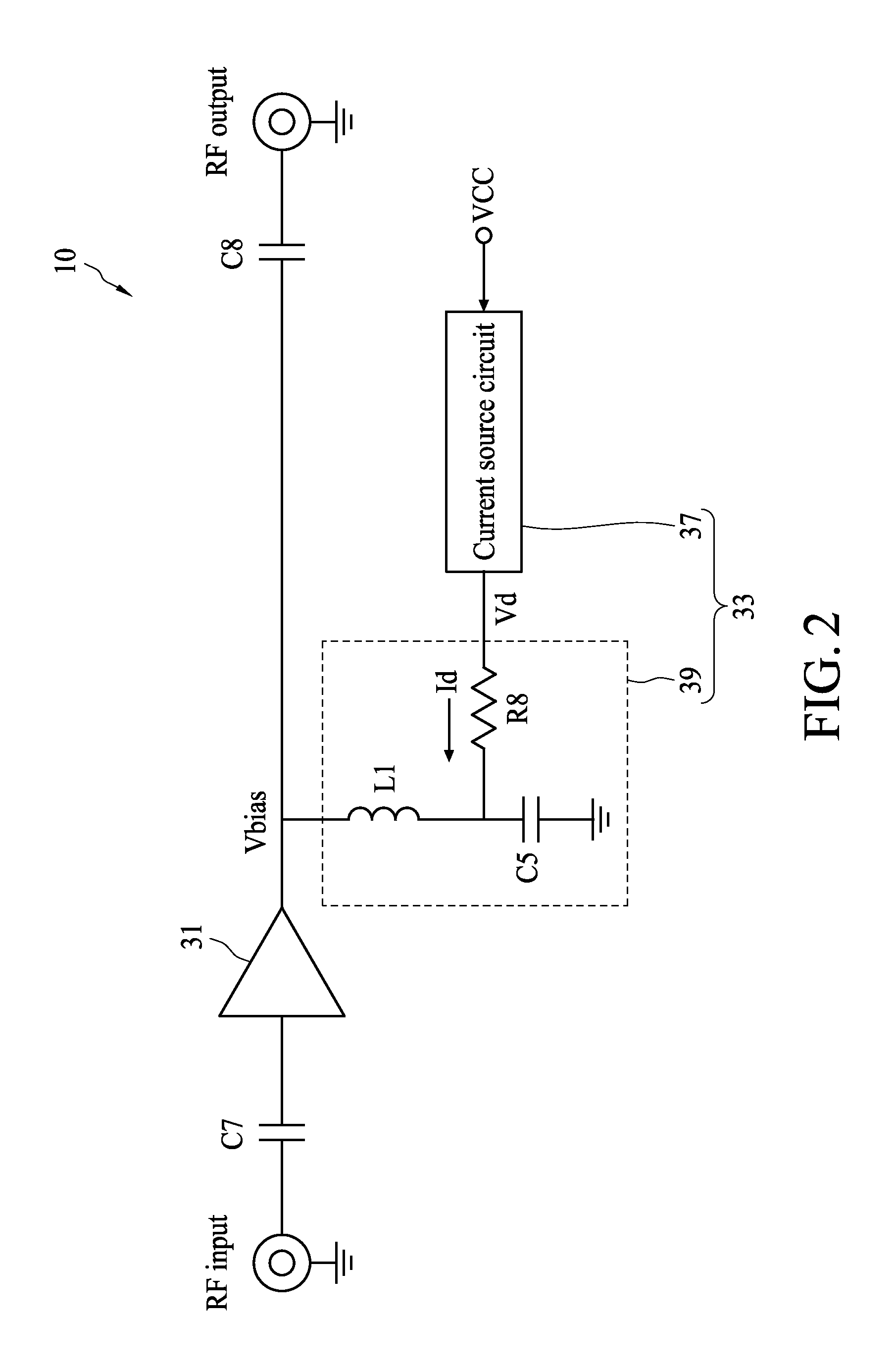
[0009]The radio frequency signal amplification system with the current source circuit according to the embodiment of the present invention can function to decrease the bias voltage (Vbias) of the MMIC gain block amplifier as the operation current (Id) increases. In addition, the curr

Problems solved by technology

However, this may also cause a disadvantage by increasing the margins of the MMIC amplifier's output power capability.
It is also possible to over-drive the final stage amplifier, and damage the final stage amplifier by outputting too much power in many abnormal operations, or system loop fails.
In such a situa

Method used


Image

  • Precise current source circuit for bias supply of RF MMIC gain block amplifier application
  • Precise current source circuit for bias supply of RF MMIC gain block amplifier application
  • Precise current source circuit for bias supply of RF MMIC gain block amplifier application

Examples


Embodiment Construction

[0023]The following description of the disclosure accompanies drawings, which are incorporated in and constitute a part of this specification, and illustrate embodiments of the disclosure, but the disclosure is not limited to the embodiments. In addition, the following embodiments can be properly integrated to complete another embodiment.

[0024]References to “one embodiment,”“an embodiment,”“exemplary embodiment,”“other embodiments,”“another embodiment,” etc. indicate that the embodiment(s) of the disclosure so described may include a particular feature, structure, or characteristic, but not every embodiment necessarily includes the particular feature, structure, or characteristic. Further, repeated use of the phrase “in the embodiment” does not necessarily refer to the same embodiment, although it may.

[0025]The term “coupled with,” along with its derivatives, may be used herein. “Coupled” may mean one or more of the following. “Coupled” may mean that two or more elements are in dire...


PUM


Abstract

A current source circuit includes a first transistor Q1, a second transistor Q2, a first resistor R1, and a second resistor R2. The first transistor Q1 has a first terminal (collector) coupled with the supply voltage (VCC), a second terminal (base) coupled with the first resistor R1, and a third terminal (emitter) coupled with the second resistor R2. The second transistor Q2 has a first terminal coupled with the second terminal of the first transistor Q1, a second terminal coupled with the third terminal of the first transistor Q1, and a third terminal coupled with the filtering circuit 39. The first resistor R1 is coupled between the supply voltage and a second terminal of the first transistor Q1. The second resistor R2 is coupled between a third terminal of the first transistor Q1 and the filtering circuit 39.

Description

FIELD OF THE INVENTION[0001]The present disclosure relates to a current source circuit, and more particularly, to a current source circuit for an MMIC gain block amplifier capable of limiting an amplifier's output power without clipping the waveform PAR, but limiting the averaged power for the MMIC gain block amplifier application, so as to prevent the occurrence of over-drive or over-power inputs to the subsequent stage amplifier.DISCUSSION OF THE BACKGROUND[0002]As the 3G / 4G wireless communication system requires high linearity and high efficiency performance on power amplifier modules, the higher power back-off designs on the front stage, or driver stage improve linearity to drive the final stage amplifier. This higher power back-off mode will operate the MMIC (Monolithic Microwave Integrated Circuit) gain block amplifier at P1 dB-10 dB or provide a more powerful back-off point on the front stage's nominal operation point in a 3G / 4G wireless communication system. Traditionally, a...

Claims


Application Information

Patent Timeline
IPC IPC(8): H03G3/20
CPCH03G3/20H03F1/302H03F3/245
Inventor LIOU, MING CHE
Owner MICROELECTRONICS TECH INC
Why Eureka
Try Eureka