Method of erasing a flash eeprom memory

a flash memory and eeprom technology, applied in static storage, digital storage, instruments, etc., can solve the problems of reducing the process of device sizing down, affecting the operation efficiency of the device, so as to reduce the vulnerability to electrical field stress induced reliability issues, the effect of shortening the duration of the biasing pulse and reducing the biasing voltag

Active Publication Date: 2009-12-17
SYNERGER INC
View PDF10 Cites 10 Cited by
  • Summary
  • Abstract
  • Description
  • Claims
  • Application Information

AI Technical Summary

Benefits of technology

[0017]As a means to avoid the problems described in prior art erase techniques, a novel erase method for flash cells is presented. One object of an embodiment of the invention is to provide a method of erasing a flash electrically erasable, programmable, read-only memory device, which allows both the usage of lower levels of biasing voltages and of shorter biasing pulse durations thus inherently having a lower vulnerability to the electrical field stress induced reliability issues.
[0022]The erase method of the present invention introduces an innovative approach for the erase process by usage of mobile positively charged traps (ions) located within the dielectric layer and of surface state traps located at the well dielectric interface. These traps assist in the erase process by serving as an intermediate point for the tunneling process. By applying the first positive voltage to the well during the first stage, these traps would be forced to deplete from any stored charge within, while during the second stage, where the well bias is reset and the control gate is inversely biased, charge is removed from the floating gate by direct and indirect, trap assisted, tunneling currents. This indirect tunneling component enables the usage of shorter bias pulses since it increases the indirect tunneling current component.
[0023]Flash cell erase is performed to a specific threshold voltage which only depends on the amount of charge removed from the floating gate. Thus, the present invention would yield higher tunneling currents without having the inevitable merits of strong electric fields exposure that usually accompany prior art methods. The present invention utilizes an electric field that is about half in magnitude then the one used in all prior art techniques and that has a shorter duration which gives higher immunity to the prior art reliability issues, which in turn have an exponential dependency on both the electric field's magnitude and duration.

Problems solved by technology

These high electrical fields are known to generate reliability issues that degrade the quality of the dielectric which would eventually cause device failure.
As devices advance further into sub micron dimensions, the intensity of the electric fields grow higher to become a dominating factor limiting the device scale down process.
This erase scheme suffers from a reliability issue caused by “hot hole” injection from the substrate 10 into the tunneling dielectric 19 [I-III].
Thus, the “hot hole” current has a strong dependency on the electric field and imposes yet another limit on device sizing as well as on operation voltage levels.
Given enough time, these traps would line up to cause a breakdown of the insulator layer and rend the device useless, a phenomena known as Time Dependent Dielectric Breakdown (TDDB).
TDDB theory presents an exponential dependency of the breakdown probability and time to failure of the device on the electrical field strength and stress duration.
Furthermore, by using NGSE the hot hole tunneling current is localized beneath the source and floating gate overlapping area and the likelihood of the dielectric traps to line up and form a breakthrough path is high.
The NGCE technique suffers from a different reliability problem.
This “hot hole” tunneling current would have the same affect on the dielectric quality and cause degradation over time.
However, since in this case, the surface states and inter dielectric traps are distributed along the entire channel length, most of the performance penalty would be manifested in cell read current degradation and reduced programming performance.
The impact on programming efficiencies results from the fact that these traps interfere with the hot carrier injection process.
This prior art technique, however, does not eliminate the need for using high electric field across the dielectric during erase and the resulting TDDB and performance degradation issues.
All prior art techniques attempt to maximize the overlap time between these waveforms in order to get the maximal electrical field during the erase sequence making them highly vulnerable to the above mentioned reliability issues.
Another drawback of this prior art operation methodology is that the biasing scheme would also yield an electric field across the control gate to floating gate dielectric that would induce charge tunneling from the former to the latter.
This tunneling current would interfere with the erase process by adding charge to the floating gate.

Method used


Image

  • Method of erasing a flash eeprom memory
  • Method of erasing a flash eeprom memory
  • Method of erasing a flash eeprom memory

Examples


Embodiment Construction

[0032]The following detailed description is meant to be illustrative only and not limiting. It is to be understood that other embodiment may be utilized and structural changes may be made without departing from the scope of the present invention. Also, it is to be understood that the phraseology and terminology used herein are for the purpose of description and should not be regarded as limiting. The use of “including,”“comprising,” or “having” and variations thereof herein is meant to encompass the items listed thereafter and equivalents thereof as well as additional items.

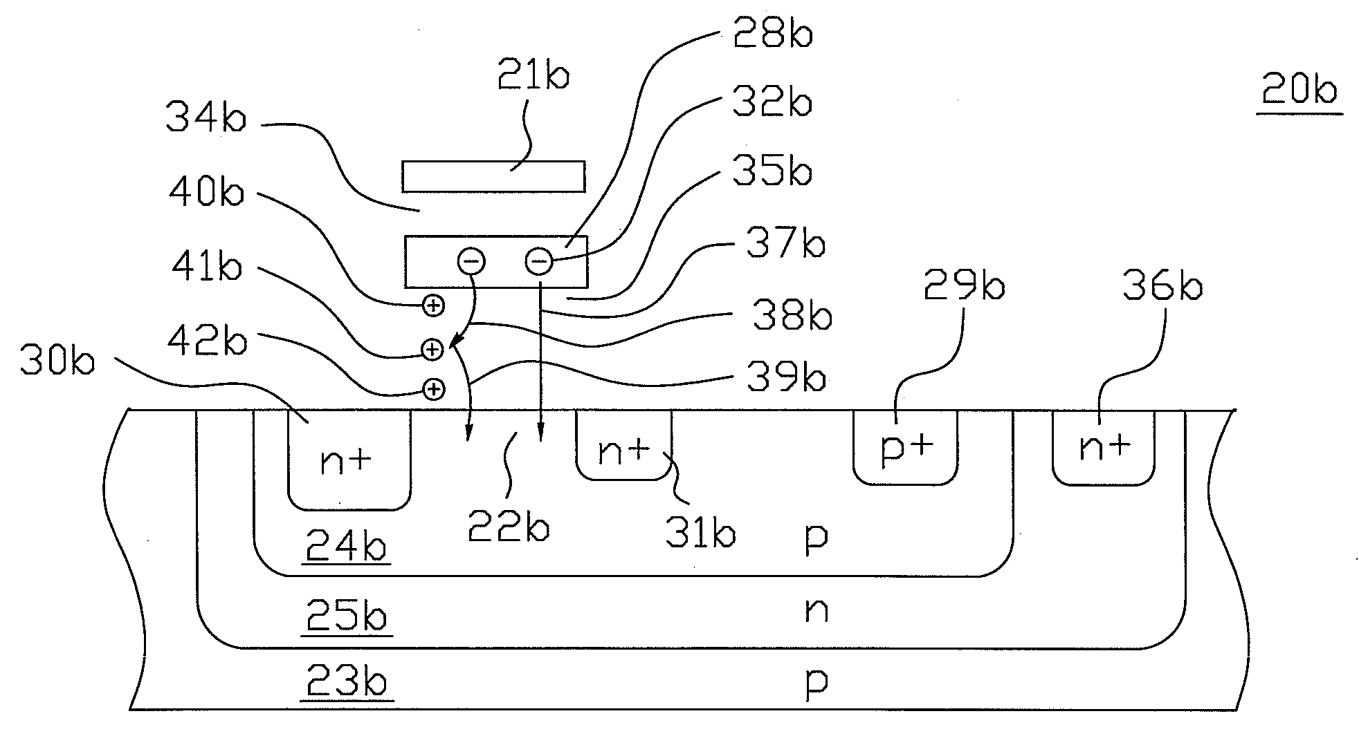
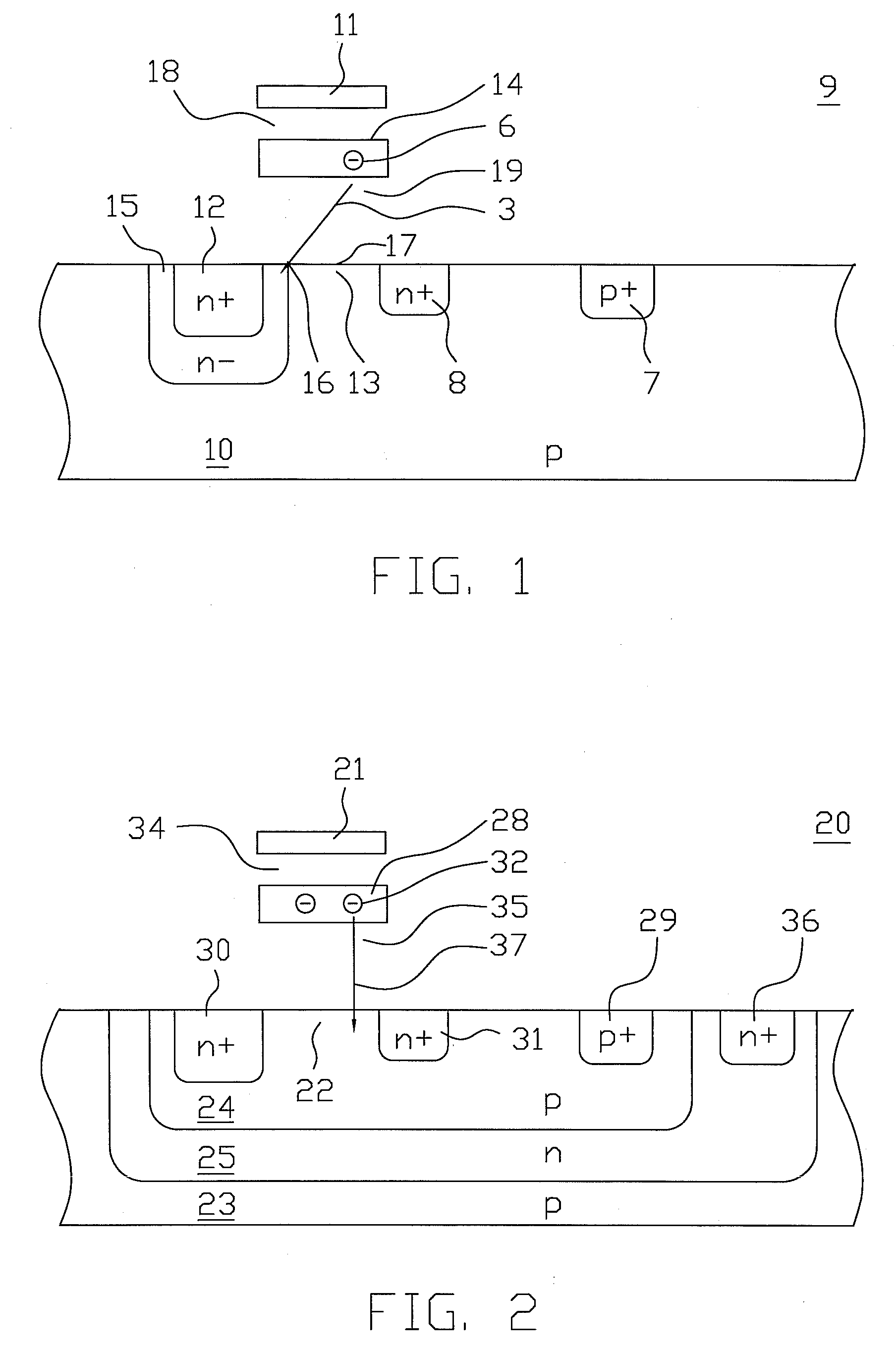
[0033]FIG. 4 shows an embodiment of the present invention using an n-type flash EEPROM. The EEPROM device 20b is formed in a p-type triple well 24b, formed within an n-type deep well 25b, formed in a p-type substrate 23b. The device has a control gate 21b that is formed above a floating gate 28b with an inter layer electrically isolating dielectric 34b. The floating gate 28b is isolated from the channel area 22b ...


PUM


Abstract

The invention is a new method for erasing a flash EEPROM memory device. The memory device has a first semiconductor region within a second semiconductor region, source and drain regions in the first semiconductor region, a well terminal inside the first semiconductor region, a charge storing layer electrically isolated from the first semiconductor region by a dielectric layer, and a control terminal electrically isolated from the charge storing layer by a inter layer dielectric. The method comprises the steps of: applying a first voltage bias of first polarity to the well terminal; allowing a first time period to elapse; applying a second voltage bias of second polarity opposite to the first polarity to the control terminal; resetting the first voltage bias to zero; allowing a second time period to elapse; and resetting the second voltage bias to zero.

Description

BACKGROUND OF THE INVENTION[0001](a) Field of the Invention[0002]This invention relates to the operation of a non volatile flash memory cell and in particular to erasing the cell by manipulating the stored charge within.[0003](b) Description of the Related Art[0004]A flash EEPROM cell is a semiconductor device having non volatile memory properties which can be electrically programmed and erased. The non volatile memory properties enable the device to retain stored information once the power is turned off. The information is in the form of electrons stored within the floating gate. Devices of this type are described in U.S. Pat. Nos. [1] 4,698,787 and [2] 5,077,691, all of which are incorporated herein by reference. Other similar devices of this type are also described in U.S. Pat. Nos. [3] 5,243,559, [4] 5,361,235, [5] 5,457,652 and [6] 5,790,460, all of which are incorporated herein by reference.[0005]Flash EEPROM devices are electrically erasable, programmable, read-only memory de...

Claims


Application Information

Patent Timeline
Patent Type & Authority Applications(United States)
IPC IPC(8): G11C16/06G11C11/34G11C7/00
CPCG11C16/14
Inventor BERCO, DANNY
Owner SYNERGER INC
Why Eureka
Try Eureka