N/P Boundary Effect Reduction for Metal Gate Transistors

a metal gate transistor and boundary effect technology, applied in the field of n/p boundary effect reduction for metal gate transistors, can solve the problems of reducing the threshold voltage (vsub>t/sub>), increasing the complexity of processing and manufacturing ics, and reducing the threshold voltage (vsub>t/sub>) of metal gate transistors. achieve significant differences in length

Active Publication Date: 2014-07-24
TAIWAN SEMICON MFG CO LTD
View PDF1 Cites 2 Cited by
  • Summary
  • Abstract
  • Description
  • Claims
  • Application Information

AI Technical Summary

Benefits of technology

[0012]One of the broader forms of the present disclosure involves a method of fabricating a semiconductor device. The method includes: forming a first dummy gate and a second dummy gate over a substrate; forming a patterned mask over the first and second dummy gates, the patterned mask exposing a first segment of the first dummy gate and a second segment of the second dummy gate, while covering a third segment of the first dummy gate and a fourth segment of the second dummy gate, wherein the forming the mask is carried out in a manner such that the first and second segments have significantly different lengths; replacing the f

Problems solved by technology

However, these advances have increased the complexity of processing and manufacturing ICs and, for these advances to be realized, similar developments in IC processing and manufacturing are needed.
However, conventional metal gate transistors may suffer from an N/P boundary effect.
Such contamination may degrade the threshold voltage (Vt) of the metal gate transistors.
Moreover, as device sizes co

Method used


Image

  • N/P Boundary Effect Reduction for Metal Gate Transistors
  • N/P Boundary Effect Reduction for Metal Gate Transistors
  • N/P Boundary Effect Reduction for Metal Gate Transistors

Examples


Embodiment Construction

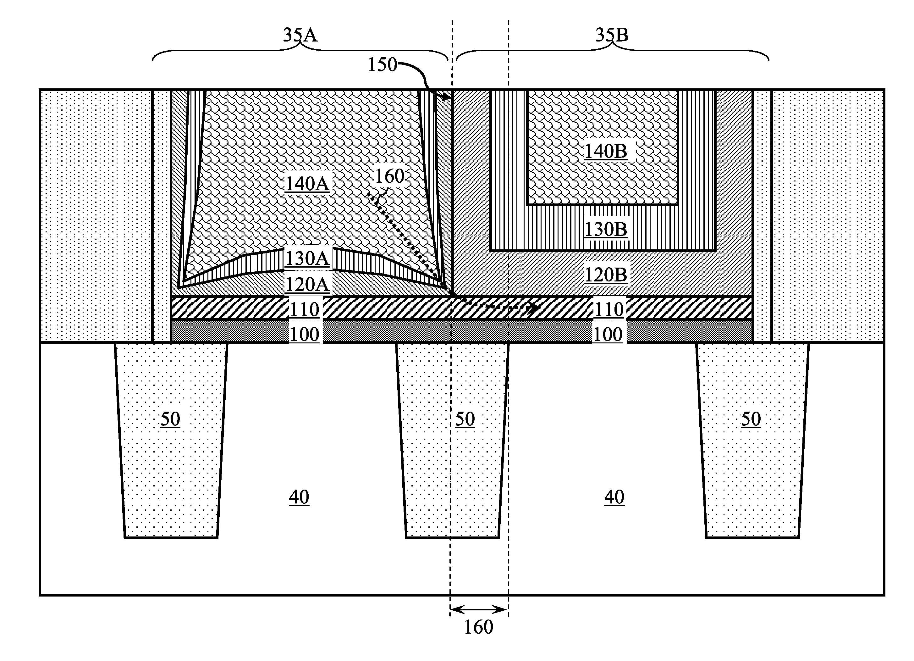
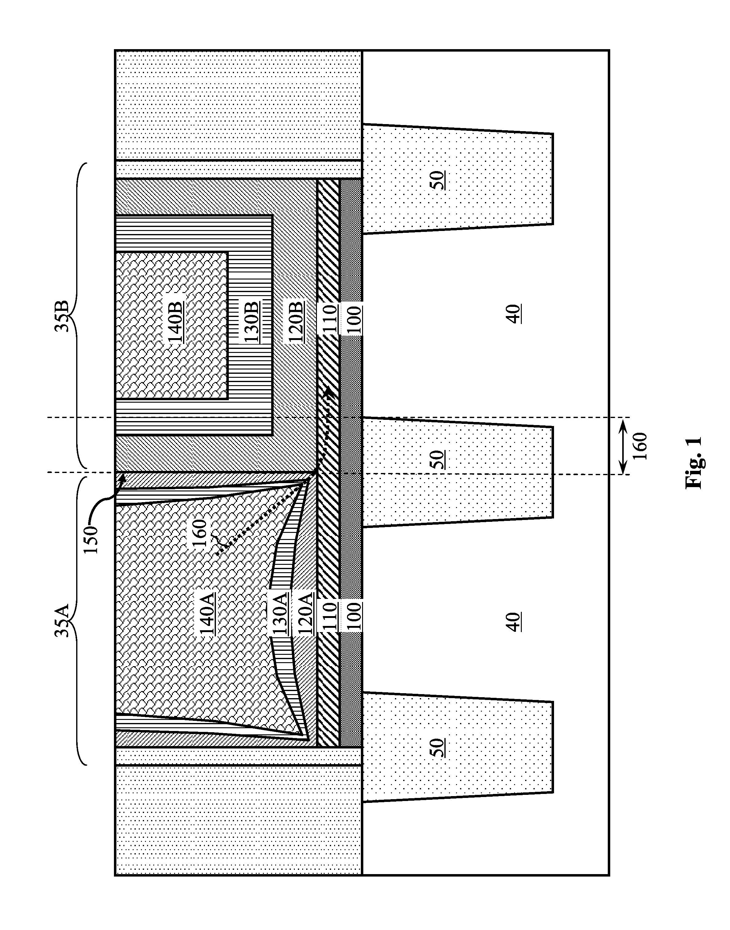
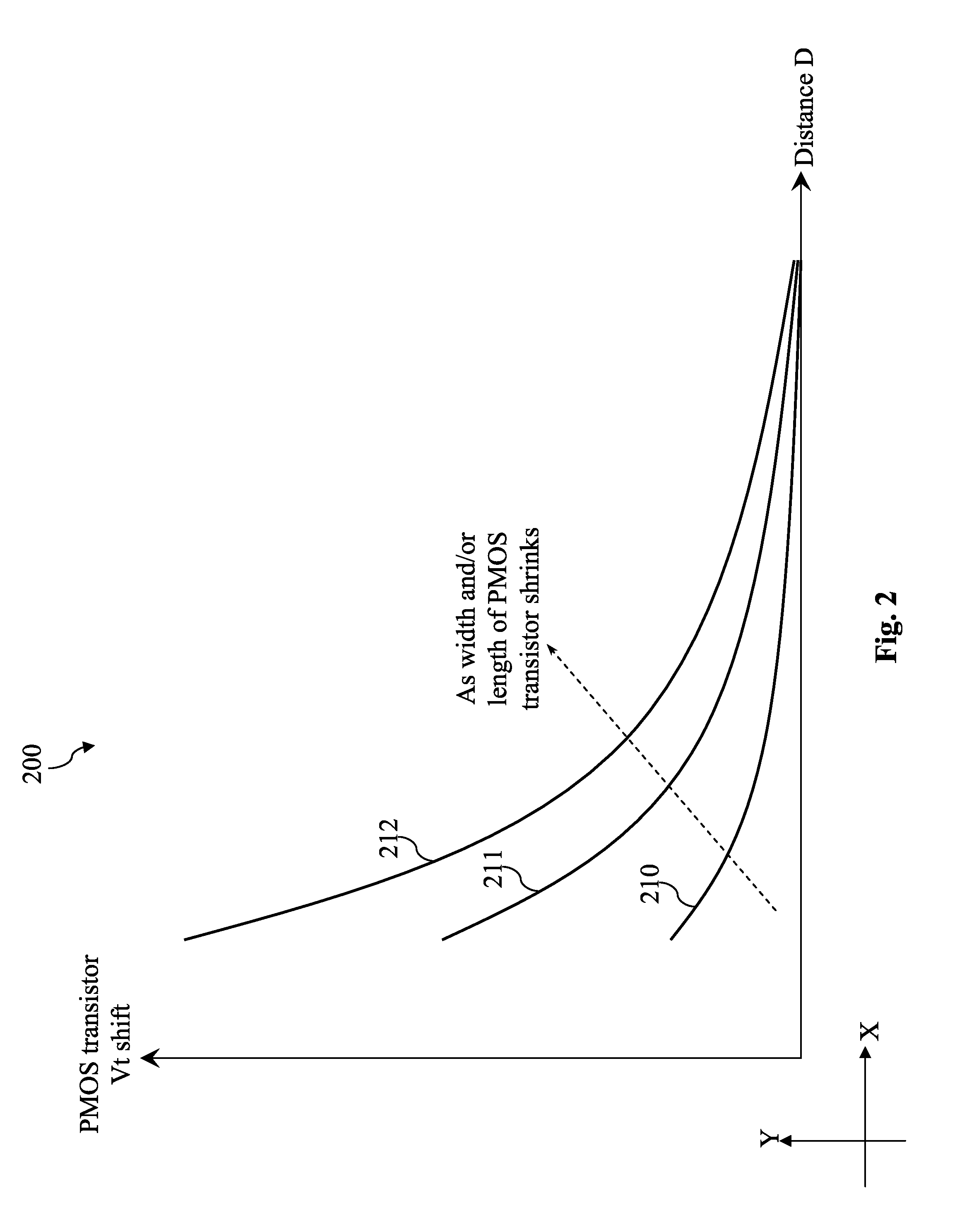
[0032]It is understood that the following disclosure provides many different embodiments, or examples, for implementing different features of various embodiments. Specific examples of components and arrangements are described below to simplify the present disclosure. These are, of course, merely examples and are not intended to be limiting. For example, the formation of a first feature over or on a second feature in the description that follows may include embodiments in which the first and second features are formed in direct contact, and may also include embodiments in which additional features may be formed between the first and second features, such that the first and second features may not be in direct contact. Moreover, the terms “top,”“bottom,”“under,”“over,” and the like are used for convenience and are not meant to limit the scope of embodiments to any particular orientation. Various features may also be arbitrarily drawn in different scales for the sake of simplicity and ...


PUM


Abstract

The present disclosure provides a method of fabricating a semiconductor device. The method includes forming a plurality of dummy gates over a substrate. The dummy gates extend along a first axis. The method includes forming a masking layer over the dummy gates. The masking layer defines an elongate opening extending along a second axis different from the first axis. The opening exposes first portions of the dummy gates and protects second portions of the dummy gates. A tip portion of the opening has a width greater than a width of a non-tip portion of the opening. The masking layer is formed using an optical proximity correction (OPC) process. The method includes replacing the first portions of the dummy gates with a plurality of first metal gates. The method includes replacing the second portions of the dummy gates with a plurality of second metal gates different from the first metal gates.

Description

PRIORITY DATA[0001]The present application is a divisional patent application of U.S. patent application Ser. No. 13 / 299,152, filed on Nov. 17, 2011, entitled “N / P Boundary Effect Reduction for Metal Gate Transistors”, the disclosure of which is hereby incorporated by reference in its entirety.BACKGROUND[0002]The semiconductor integrated circuit (IC) industry has experienced rapid growth. Technological advances in IC materials and design have produced generations of ICs where each generation has smaller and more complex circuits than the previous generation. However, these advances have increased the complexity of processing and manufacturing ICs and, for these advances to be realized, similar developments in IC processing and manufacturing are needed. In the course of integrated circuit evolution, functional density (i.e., the number of interconnected devices per chip area) has generally increased while geometry size (i.e., the smallest component (or line) that can be created using...

Claims


Application Information

Patent Timeline
IPC IPC(8): H01L29/423H01L27/092
CPCH01L21/0274H01L21/823456H01L21/32139H01L27/0207H01L21/28123H01L29/4966H01L29/513H01L29/517H01L29/66545H01L27/092H01L29/42356H01L29/41775
Inventor CHUANG, HARRY HAK-LAYKUO, CHENG-CHENGTSAI, CHING-CHEZHU, MINGYOUNG, BAO-RU
Owner TAIWAN SEMICON MFG CO LTD
Why Eureka
Try Eureka