Hybrid multi-spectrum photosensitive pixel group, photosensitive device, and photosensitive system

a multi-spectrum, light-sensing technology, applied in the field of light-sensing, can solve the problems of only about 50% of semiconductor quantum efficiency and greatly limited infrared induction, and achieve the effects of high light-sensing sensitivity, high light-sensing sensitivity, and convenient surface machining

Active Publication Date: 2014-07-31
BOLY MEDIA COMM SHENZHEN
View PDF3 Cites 27 Cited by
  • Summary
  • Abstract
  • Description
  • Claims
  • Application Information

AI Technical Summary

Benefits of technology

[0064]Beneficial effects of the mixed multi-spectrum light-sensing pixel group, the light-sensing device and the system of the present invention lie in that: the chemical coating light-sensing pixel and the semiconductor light-sensing pixel have their respective advantages and disadvantages. Benefits of the chemical coating light-sensing pixel are in that the light-sensing sensitivity is high (particularly for the infrared light part), and the surface machining is convenient, but an additional semiconductor reading layer and a light filtering film are required (to obtain a color). The semiconductor light-sensing pixel does not need an additional semiconductor reading layer, but a problem of balance between light-sensing sensitivity and manufacturing difficulty exists. In the present invention, the chemical coating light-sensing pixel and the semiconductor light-sensing pixel are organically combined, and can learn strong points from each other to offset respective weaknesses, no additional semiconductor reading layer or light filtering film needs to be disposed, the difficulty of manufacturing the semiconductor light-sensing pixel is not increased, and high light-sensing sensitivity is provided, thereby exploiting respective advantages to the full; numerous color signals and other spectral signals may be simultaneously obtained, energy of incident photons can be maximally utilized, and the theoretical upper limit of photoelectric conversion efficiency is achieved or approximately achieved; colors may be completely reconstructed, and meanwhile images of other spectrums including an ultraviolet image, a near-infrared image, and a far-infrared image are obtained.

Problems solved by technology

These new technologies and inventions enormously improve performances and application manners of a semiconductor light-sensing device, but are still subjected to two basic limitations of the semiconductor light-sensing device itself: (1) the bandgap is small, so that infrared induction is greatly limited; and (2) the semiconductor quantum efficiency is only about 50%.

Method used


Image

  • Hybrid multi-spectrum photosensitive pixel group, photosensitive device, and photosensitive system
  • Hybrid multi-spectrum photosensitive pixel group, photosensitive device, and photosensitive system
  • Hybrid multi-spectrum photosensitive pixel group, photosensitive device, and photosensitive system

Examples


Embodiment Construction

[0093]The present invention is further illustrated in detail below through specific implementation manners with reference to accompanying drawings.

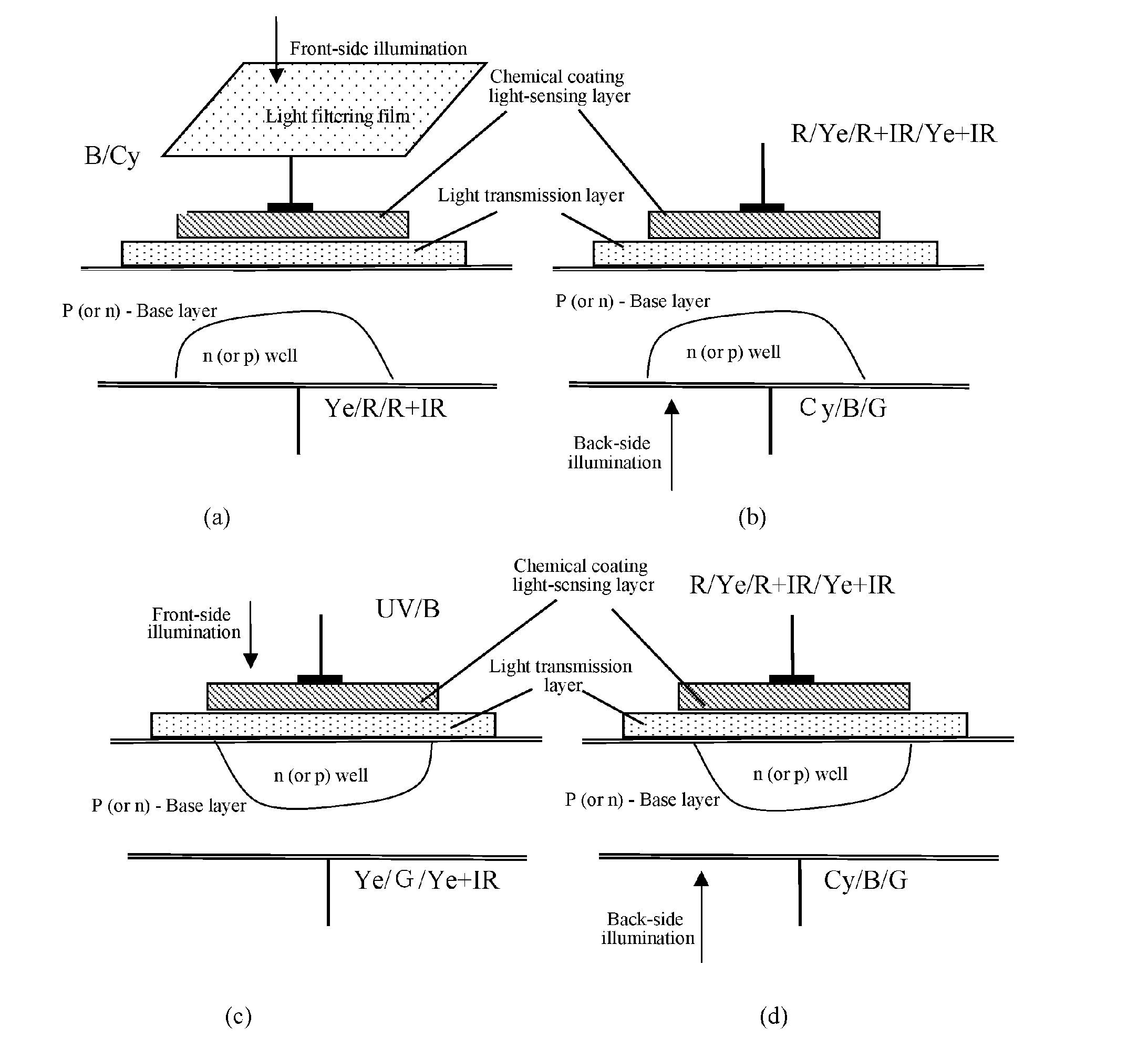
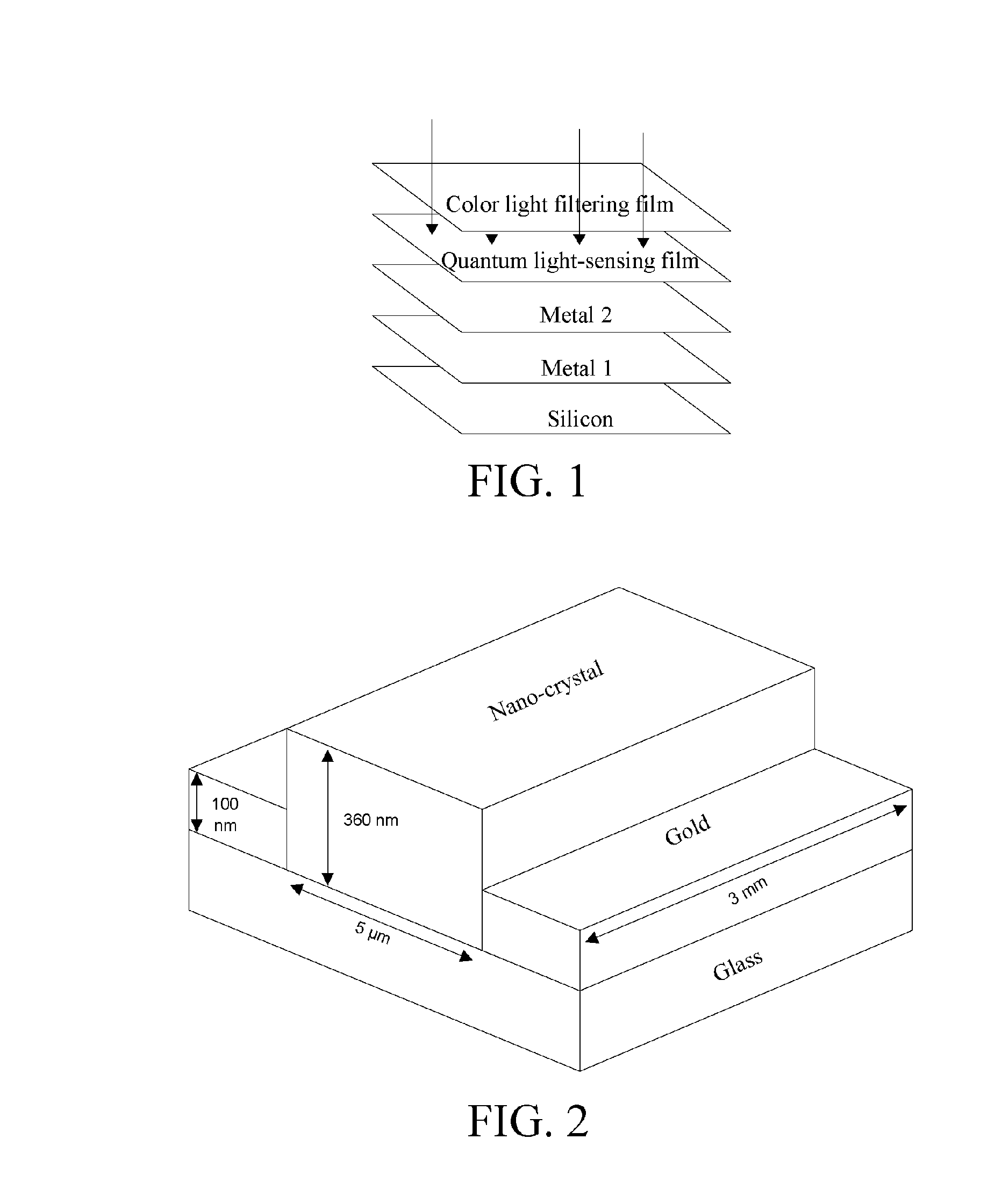
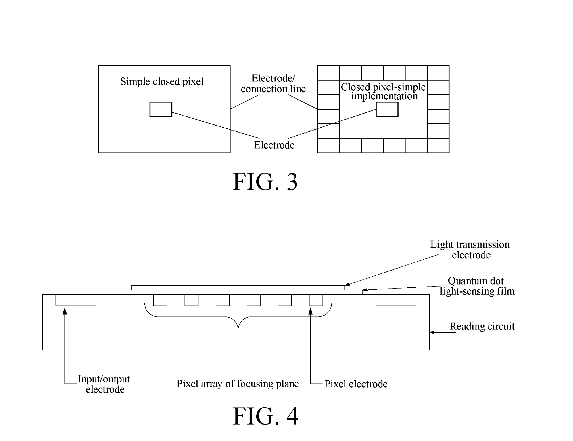
[0094]The present invention relates to a light-sensing device, and in particular, to design, manufacturing, and system use of a large-array high-performance multi-spectrum light-sensing device. The present invention merges a novel technology for a quantum dot light-sensing film or another possible chemical coating light-sensing pixel and a mature semiconductor light-sensing chip technology, to invent a new mixed light-sensing device and a system thereof, which combine to advantages of a semiconductor (CCD or CMOS) light-sensing device and a chemical coating (such as, quantum film) light-sensing device, so as to obtain a multi-spectrum light-sensing device which achieves or almost achieves the theoretical limit of light use efficiency.

[0095]In an implementation manner of the present invention, firstly a mixed multi-spectrum light-sensing p...


PUM


Abstract

The present invention relates to a mixed multi-spectrum light-sensing pixel group, a light-sensing device, and a light-sensing system. The mixed multi-spectrum light-sensing pixel group includes at least one chemical coating light-sensing pixel and at least one semiconductor light-sensing pixel. In the present invention, the chemical coating light-sensing pixel and the semiconductor light-sensing pixel are combined to generate a mixed multi-spectrum light-sensing pixel, numerous color signals and other spectral signals may be simultaneously obtained, energy of incident photons can be maximally utilized, and the theoretical upper limit of photoelectric conversion efficiency is achieved or approximately achieved; colors may be completely reconstructed, and meanwhile images of other spectrums including an ultraviolet image, a near-infrared image, and a far-infrared image are obtained.

Description

BACKGROUND OF THE INVENTION[0001]1. Field of the Invention[0002]The present invention relates to the light-sensing field, and specifically, to a mixed multi-spectrum light-sensing pixel group, a light-sensing device, and a light-sensing system.[0003]2. Related Art[0004]The present invention is continuation to “multi-spectrum light-sensing device and manufacturing method for same” (PCT / CN2007 / 071262), “multi-spectrum light-sensing device and manufacturing method for same” (Chinese Application No: 200810217270.2), “multi-spectrum light-sensing device” (Chinese Application No: 200910105372.X), “multi-spectrum light-sensing device and sampling method for same” (Chinese Application No: 200910105948.2), and “light-sensing device and reading method for same, and reading circuit” (Chinese Application No: 200910106477.7) applied by the inventor at an earlier time, aiming to provide more specific and preferable implementation at a chip and system grade.[0005]The present inventions listed abov...

Claims


Application Information

Patent Timeline
Patent Type & Authority Applications(United States)
IPC IPC(8): H01L31/0352H01L27/144
CPCH01L27/14621H01L27/14641H01L27/14647H01L31/0352H01L27/14652H01L27/1443H01L31/035218H01L27/14625H10K39/32
Inventor HU, XIAOPING
Owner BOLY MEDIA COMM SHENZHEN
Why Eureka
Try Eureka