Controlled metal extrusion opening in semiconductor structure and method of forming

a metal extrusion and semiconductor technology, applied in semiconductor devices, semiconductor/solid-state device details, capacitors, etc., can solve the problems of slots or voids may not prevent shorting in the circuit, and shorting of active circuit areas within the semiconductor structur

Inactive Publication Date: 2014-09-04
ALSEPHINA INNOVATIONS INC
View PDF2 Cites 5 Cited by
  • Summary
  • Abstract
  • Description
  • Claims
  • Application Information

AI Technical Summary

Problems solved by technology

These extrusions may form on the sidewalls of the semiconductor structure, and may result in shorting of an active circuit area within the semiconductor structure.
However, dependent on the exposure to the high temperature during the metal annealing process, the metal layer may still form extrusions that short the active circuit area.
That is, the slots or voids may not prevent shorting in the circuit, especially in the semiconductor structure which includes a small island circuit.
However, by making the slots or voids larger, the size of the active circuit becomes larger, which results in a larger semiconductor structure.
Electronic devices utilizing a larger semiconductor structure may require new design of the circuitry and / or may require a larger overall size, which is undesirable.

Method used


Image

  • Controlled metal extrusion opening in semiconductor structure and method of forming
  • Controlled metal extrusion opening in semiconductor structure and method of forming
  • Controlled metal extrusion opening in semiconductor structure and method of forming

Examples


Embodiment Construction

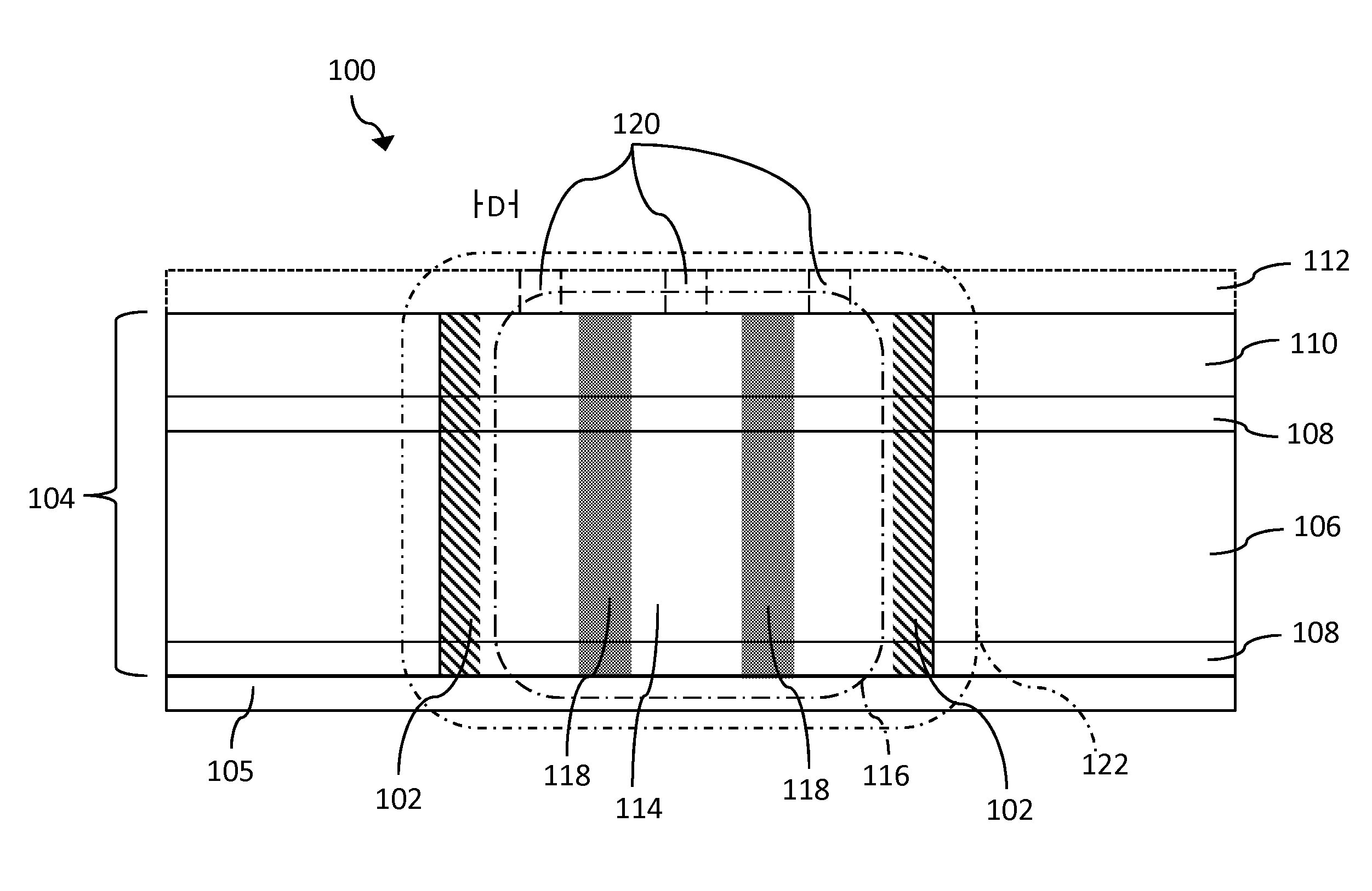
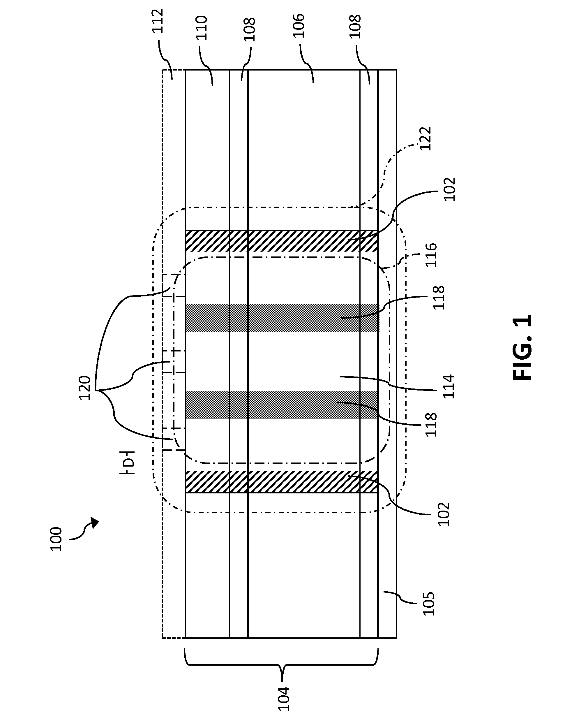
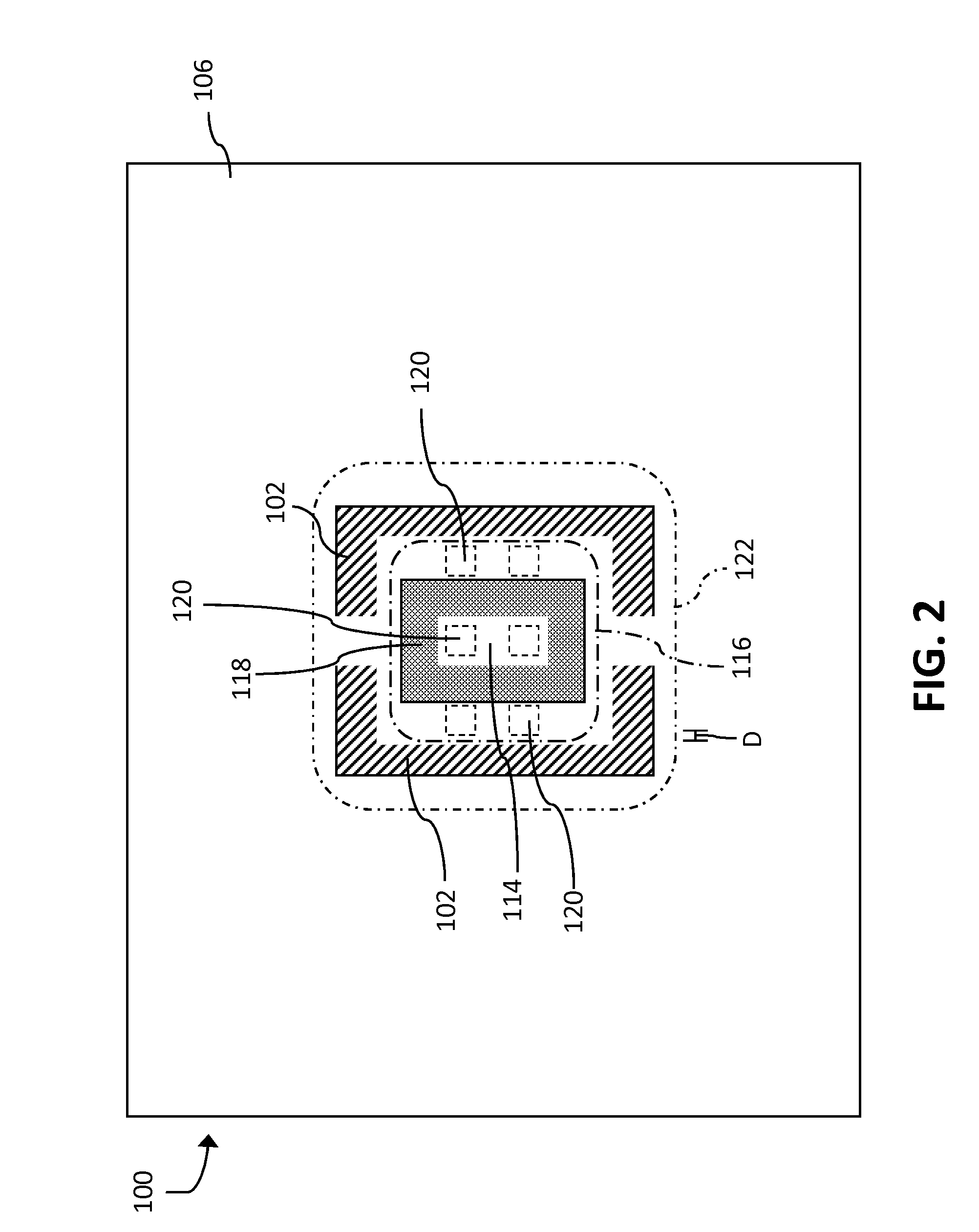
[0018]As described herein, aspects of the invention relate to a controlled metal extrusion opening in a semiconductor structure and method of forming. Specifically, as described herein, aspects of the invention related to a semiconductor structure including a plurality of openings for receiving a lateral extrusion of the aluminum layer during a metal annealing process of the semiconductor structure.

[0019]Turning to FIG. 1 a cross-sectional view of a portion of a semiconductor structure 100 is shown including lateral extrusion receiving openings 102 prior to a metal annealing process according to various embodiments of the invention. As shown in FIG. 1, and as discussed herein, semiconductor structure 100 may include a metal-insulator-metal (MIM) capacitor (not shown) and specifically, the portion of semiconductor structure 100 may include a metallurgy stack 104 which may act as a bottom plate for a MIM capacitor.

[0020]As shown in FIG. 1, metallurgy stack 104 of semiconductor structu...


PUM

PropertyMeasurementUnit
semiconductoraaaaaaaaaa
distanceaaaaaaaaaa
semiconductor structureaaaaaaaaaa

Abstract

Aspects of the present invention relate to a controlled metal extrusion opening in a semiconductor structure. Various embodiments include a semiconductor structure. The structure includes an aluminum layer. The aluminum layer includes an aluminum island within the aluminum layer, and a lateral extrusion receiving opening extending through the aluminum layer adjacent the aluminum island. The opening includes a lateral extrusion of the aluminum layer of the semiconductor structure. Additional embodiments include a method of forming a semiconductor structure. The method can include forming an aluminum layer over a titanium layer. The aluminum layer includes an aluminum island within the aluminum layer. The method can also include forming an opening extending through the aluminum layer adjacent the aluminum island within the aluminum layer. The opening includes a lateral extrusion of the aluminum layer of the semiconductor layer.

Description

BACKGROUND[0001]1. Technical Field[0002]The subject matter disclosed herein is related generally to semiconductor structures. More particularly, the subject matter disclosed herein relates to a controlled metal extrusion opening in a semiconductor structure and method of forming.[0003]2. Related Art[0004]The layers of material forming a semiconductor structure undergo a variety of physical changes during the formation of the semiconductor structure. For example, during a metal annealing process, the metal layers of the semiconductor structure may be exposed to high temperatures for an extended period of time, and may also experience a compression force from the layers of the semiconductor positioned above the metal layers. Due to the high temperature and / or compression force, some of the metal layers of the semiconductor structure may form extrusions during the metal annealing process. These extrusions may form on the sidewalls of the semiconductor structure, and may result in short...

Claims


Application Information

Patent Timeline
Patent Type & Authority Applications(United States)
IPC IPC(8): H01L23/482H01L21/768
CPCH01L21/76883H01L23/482H01L2924/0002H01L28/60H01L23/5223H01L23/528H01L23/53223H01L2924/00H01L23/5283H01L23/53214
Inventor LEVY, MAX G.MILO, GARY L.MOON, MATTHEW D.SPERANZA, ANTHONY C.SULLIVAN, TIMOTHY D.THOMAS, DAVID C.WILLIAMS, STEVEN S.
Owner ALSEPHINA INNOVATIONS INC
Why Eureka
Try Eureka